
Network Device User Guide


Device User Guide — 9S12C128DGV1/D V01.05
15
Preface
The Device User Guide provides information about the MC9S12C-Family as well the MC9S12GC-Family
devices made up of standard HCS12 blocks and the HCS12 processor core. This document is part of the
customer documentation. A complete set of device manuals also includes the HCS12 Core User Guide and
all the individual Block User Guides of the implemented modules. In an effort to reduce redundancy all
module specific information is located only in the respective Block User Guide. If applicable, special
implementation details of the module are given in the block description sections of this document.
The C-Family and the GC-Family offer an extensive range of package, temperature and speed options.
The members of the GC-Family do not feature a CAN module.
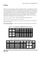
Table 0-1 shows a feature overview of the MC9S12C and MC9S12GC Family members.
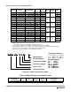
Table 0-2 summarizes the package option and size configuration.
Table 0-3 lists the part number coding based on the package, speed and temperature and preliminary die
options for the C-Family.
Table 0-4 lists the part number coding based on the package, speed and temperature and preliminary die
options for the GC-Family.
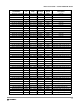
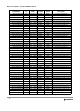
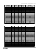
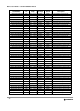
Table 0-2 MC9S12C-Family Package Option Summary
Table 0-1 List of MC9S12C and MC9S12GC Family members
Flash RAM Device CAN SCI SPI A/D PWM Timer
128K 4K
MC9S12C128 1 1 1 8ch 6ch 8ch
MC9S12GC128 — 1 1 8ch 6ch 8ch
96K 4K MC9S12C96 1 1 1 8ch 6ch 8ch
64K 4K
MC9S12C64 1 1 1 8ch 6ch 8ch
MC9S12GC64 — 1 1 8ch 6ch 8ch
32K 2K
MC9S12C32 1 1 1 8ch 6ch 8ch
MC9S12GC32 — 1 1 8ch 6ch 8ch
16K 1K MC9S12GC16 — 1 1 8ch 6ch 8ch
Package Device Part Number
Mask
1
set
Temp.
2
Options
Flash RAM
I/O
3
,
4
48LQFP MC9S12C128 MC9S12C128 0L09S M, V, C
128K 4K
31
52LQFP MC9S12C128 MC9S12C128 0L09S M, V, C 35
80QFP MC9S12C128 MC9S12C128 0L09S M, V, C 60
48LQFP MC9S12C96 MC9S12C96 TBD M, V, C
96K 4K
31
52LQFP MC9S12C96 MC9S12C96 TBD M, V, C 35
80QFP MC9S12C96 MC9S12C96 TBD M, V, C 60