
Network Device User Guide


Device User Guide — 9S12C128DGV1/D V01.05
120
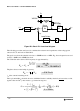
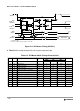
Figure C-2 SPI Master Timing (CPHA=1)
In Table C-2 the timing characteristics for master mode are listed.
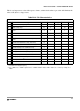
Table C-2 SPI Master Mode Timing Characteristics
Num C Characteristic Symbol Unit
Min Typ Max
1 P SCK Frequency
f
sck
1/2048 — 1/2
f
bus
1 P SCK Period
t
sck
2 — 2048
t
bus
2 D Enable Lead Time
t
lead
— 1/2 —
t
sck
3 D Enable Lag Time
t
lag
— 1/2 —
t
sck
4 D Clock (SCK) High or Low Time
t
wsck
— 1/2 —
t
sck
5 D Data Setup Time (Inputs)
t
su
8— — ns
6 D Data Hold Time (Inputs)
t
hi
8— — ns
9 D Data Valid after SCK Edge
t
vsck
— — 30 ns
10 D Data Valid after
SS fall (CPHA=0)
t
vss
— — 15 ns
11 D Data Hold Time (Outputs)
t
ho
20 — — ns
12 D Rise and Fall Time Inputs
t
rfi
—— 8 ns
13 D Rise and Fall Time Outputs
t
rfo
—— 8 ns
SCK
(OUTPUT)
SCK
(OUTPUT)
MISO
(INPUT)
MOSI
(OUTPUT)
1
5 6
MSB IN
2
BIT 6 . . . 1
LSB IN
MASTER MSB OUT
2
MASTER LSB OUT
BIT 6 . . . 1
4
4
9
12 13
11
PORT DATA
(CPOL
=
0)
(CPOL
=
1)
PORT DATA
SS
1
(OUTPUT)
2
12 13 3
1.If configured as output
2. LSBF = 0. For LSBF = 1, bit order is LSB, bit 1, ..., bit 6, MSB.