
Network Device User Guide
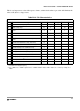


Device User Guide — 9S12C128DGV1/D V01.05
112
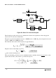
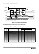
Figure B-3 Basic PLL functional diagram
The following procedure can be used to calculate the resistance and capacitance values using typical
values for K
1
, f
1
and i
ch
from Table B-12.
The grey boxes show the calculation for f
VCO
= 50MHz and f
ref
= 1MHz. E.g., these frequencies are used
for f
OSC
= 4MHz and a 25MHz bus clock.
The VCO Gain at the desired VCO frequency is approximated by:
The phase detector relationship is given by:
i
ch
is the current in tracking mode.
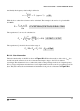
The loop bandwidth f
C
should be chosen to fulfill the Gardner’s stability criteria by at least a factor of 10,
typical values are 50. ζ = 0.9 ensures a good transient response.
f
osc
1
refdv+1
f
ref
Phase
Detector
VCO
K
V
1
synr+1
f
vco
Loop Divider
K
Φ
1
2
∆
f
cmp
C
s
R
C
p
VDDPLL
XFC Pin
K
V
K
1
e
f
1
f
vco
–()
K
1
1V⋅
-----------------------
⋅=
100– e
60 50–()
100–
------------------------
⋅=
= -90.48MHz/V
K
Φ
i
ch
– K
V
⋅=
= 316.7Hz/Ω
f
C
2 ζ f
ref
⋅⋅
πζ 1 ζ
2
++
⋅
------------------------------------------
1
10
------
f
C
f
ref
410⋅
-------------- ζ 0.9=();<→<
f
C
< 25kHz