
Network Device User Guide


Device User Guide — 9S12C128DGV1/D V01.05
111
time t
UPOSC
. The device features a clock monitor. A time-out is asserted if the frequency of the incoming
clock signal is below the Clock Monitor FailureAssert Frequency f
CMFA.
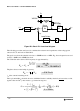
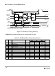
B.6.3 Phase Locked Loop
The oscillator provides the reference clock for the PLL. The PLL´s Voltage Controlled Oscillator (VCO)
is also the system clock source in self clock mode.
B.6.3.1 XFC Component Selection
This section describes the selection of the XFC components to achieve a good filter characteristics.
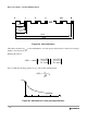
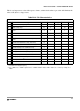
Table B-11 Oscillator Characteristics
Conditions are shown in Table A-4 unless otherwise noted
Num C Rating Symbol Min Typ Max Unit
1a C Crystal oscillator range (Colpitts)
f
OSC
0.5 16 MHz
1b C
Crystal oscillator range (Pierce)
1(4)
NOTES:
1. Depending on the crystal a damping series resistor might be necessary
f
OSC
0.5 40 MHz
2 P Startup Current
i
OSC
100 µA
3 C Oscillator start-up time (Colpitts)
t
UPOSC
8
2
2. f
osc
= 4MHz, C = 22pF.
100
3
3. Maximum value is for extreme cases using high Q, low frequency crystals
ms
4 D Clock Quality check time-out
t
CQOUT
0.45 2.5 s
5 P Clock Monitor Failure Assert Frequency
f
CMFA
50 100 200 KHz
6P
External square wave input frequency
4
4. XCLKS =0 during reset
f
EXT
0.5 50 MHz
7 D External square wave pulse width low
t
EXTL
9.5 ns
8 D External square wave pulse width high
t
EXTH
9.5 ns
9 D External square wave rise time
t
EXTR
1ns
10 D External square wave fall time
t
EXTF
1ns
11 D Input Capacitance (EXTAL, XTAL pins)
C
IN
7pF
12 C
DC Operating Bias in Colpitts Configuration
on EXTAL Pin
V
DCBIAS
1.1 V