
Network Device User Guide


Device User Guide — 9S12C128DGV1/D V01.05
100
beyond the power supply levels that it ties to. If the input level goes outside of this range it will effectively
be clipped
B.4.3 Factors influencing accuracy
Three factors - source resistance, source capacitance and current injection - have an influenceon the
accuracy of the ATD.
B.4.3.1 Source Resistance:
Due to the input pin leakage current as specified in Table A-6 in conjunction with the source resistance
there will be a voltage drop from the signal source to the ATD input. The maximum source resistance R
S
specifies results in an error of less than 1/2 LSB (2.5mV) at the maximum leakage current. If device or
operating conditions are less than worst case or leakage-induced error is acceptable, larger values of source
resistance is allowable.
B.4.3.2 Source capacitance
When sampling an additional internal capacitor is switched to the input. This can cause a voltage drop due
to charge sharing with the external and the pin capacitance. For a maximum sampling error of the input
voltage ≤ 1LSB, then the external filter capacitor, C
f
≥ 1024 * (C
INS
- C
INN
).
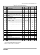
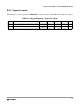
Table B-4 ATD Operating Characteristics
Conditions are shown in Table A-4 unless otherwise noted; Supply Voltage 3.3V-10% <= V
DDA
<= 3.3V+10%
Num C Rating Symbol Min Typ Max Unit
1D
Reference Potential
Low
High
V
RL
V
RH
V
SSA
V
DDA
/2
V
DDA
/2
V
DDA
V
V
2 C Differential Reference Voltage
V
RH
-V
RL
3.0 3.3 3.6 V
3 D ATD Clock Frequency
f
ATDCLK
0.5 2.0 MHz
4D
ATD 10-Bit Conversion Period
Clock Cycles
1
Conv, Time at 2.0MHz ATD Clock f
ATDCLK
NOTES:
1. The minimum time assumes a final sample period of 2 ATD clocks cycles while the maximum time assumes a final sample
period of 16 ATD clocks.
N
CONV10
T
CONV10
14
7
28
14
Cycles
µs
5D
ATD 8-Bit Conversion Period
Clock Cycles
(1)
Conv, Time at 2.0MHz ATD Clock f
ATDCLK
N
CONV8
T
CONV8
12
6
26
13
Cycles
µs
6D
Recovery Time (V
DDA
=3.3 Volts)
t
REC
20 µs
7 P Reference Supply current
I
REF
0.250 mA