
MC68VZ328 Integrated Processor User's Manual
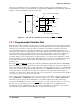


Programming Model
Chip-Select Logic 6-11
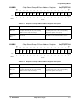
WS3–1
Bits 6–4
Wait State—This field determines the
number of wait states added before an
internal DTACK signal is returned for this
chip-select.
Note: When using the external DTACK
signal, you must configure the
BUSW/DTACK
/PG0 pin.
000 = 0 + WS0 wait states.
001 = 2 + WS0 wait states.
010 = 4 + WS0 wait states.
011 = 6 + WS0 wait states.
100 = 8 + WS0 wait states.
101 = 10 + WS0 wait states.
110 = 12 + WS0 wait states.
111 = External DTACK.
When using the external DTACK
signal, you must
select DTACK
function in Port G.
WS0 is the DWS0, CWS0, BWS0, or AWS0 bit in the
CSCTRL1 register.
SIZ
Bits 3–1
Chip-Select Size—This field determines
the memory range of the chip-select. For
CSAx
and CSBx, the chip-select size is
between 128K and 16 Mbyte. For CSCx
and CSDx
, the chip-select size is between
32K and 16 Mbyte.
000 = 128K (32K or 8 Mbyte* for CSCx
and CSDx).
001 = 256K (64K or 16 Mbyte* for CSCx
and CSDx).
010 = 512K (128K for CSCx
and CSDx).
011 = 1 Mbyte (256K for CSCx
and CSDx).
100 = 2 Mbyte (512K for CSCx
and CSDx).
101 = 4 Mbyte (1 Mbyte for CSCx
and CSDx).
110 = 8 Mbyte (2 Mbyte for CSCx
and CSDx).
111 = 16 Mbyte (4 Mbyte for CSCx
and CSDx).
* Note: Large DRAM size selection requires the DSIZ3
bit in the chip-select control register to be set.
EN
Bit 0
Chip-Select Enable—This write-only bit
enables each chip-select.
0 = Disabled.
1 = Enabled.
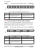
Table 6-8. Chip-Select Register B Description (Continued)
Name Description Setting