
MC68VZ328 Integrated Processor User's Manual


5-6 MC68VZ328 User’s Manual
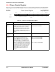
Programming Model
5.2.4 I/O Drive Control Register
This register controls the driving strength of all I/O signals. By default, all pins are defaulted to 4 mA
driving current. After reset, system software should select 2 mA driving for those signals that do not need
high-current driving for power saving. The bit assignments for the register are shown in the following
display. The settings for the bits in the register are listed in Table 5-4.
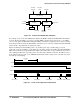
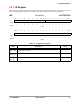
IODCR I/O Drive Control Register 0x(FF)FFF008
BIT 1514 13 12 11 10 987654321BIT 0
AB DB CB PM PK PJ PG PF PE PD PC PB PA
TYPE
rw rw rw rw rw rw rw rw rw rw rw rw rw
RESET
0 0 0 1 1 1 1111111111
0x1FFF
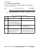
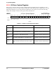
Table 5-4. I/O Drive Control Register Description
Name Description Setting
Reserved
Bits 15–13
Reserved Do not use these bits.
AB
Bit 12
Address Bus Signals I/O Drive Control—It should be
noted that A[23:20] are controlled by the PF bit.
0 = I/O drive current for each pin is 2 mA.
1 = I/O drive current for each pin is 4 mA.
DB
Bit 11
Upper Data Bus Signals I/O Drive Control—The
lower data bus is controlled by the PA bit.
0 = I/O drive current for each pin is 2 mA.
1 = I/O drive current for each pin is 4 mA.
CB
Bit 10
Control Bus Signals—Only those signals or functions
not multiplexed with GPIO are controlled by this bit.
0 = I/O drive current for each pin is 2 mA.
1 = I/O drive current for each pin is 4 mA.
PM–PA
Bits 9–0
Port M to Port A Group I/O Drive Control—Each bit
controls the drive current for the lines in the respective
port.
0 = I/O drive current for each pin is 2 mA.
1 = I/O drive current for each pin is 4 mA.