
MC68VZ328 Integrated Processor User's Manual
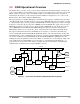


CGM Programming Model
Clock Generation Module and Power Control Module 4-9
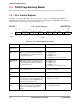
DISPLL
Bit 3
Disable PLL—This bit, when set, disables the
output of the PLL, placing the chip in sleep
mode, its lowest power state.
0 = PLL enabled (default).
1 = PLL disabled.
Reserved
Bit 2
Reserved This bit is reserved and should be set to 0.
WKSEL
Bits 1–0
Wake-up Clock Select—This field selects the
delay of the PLL output from the initiation of
the wake up until an output is available. Since
the delay time is calculated by counting CLK32
cycles, the frequency of the crystal oscillator
will determine the amount of delay that each
setting produces.
See Table 4-3 for delay settings.
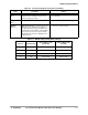
Table 4-3. WKSEL Field (PLLCR) Delay Settings
Bits 1–0 CLK32 Periods
Delay in Milliseconds
(32.768 kHz)
Delay in Milliseconds
(38.4 kHz)
00 32 0.976 0.833
01 48 1.465 1.250
10 64 1.953 1.667
11 96 2.93 (default) 2.500 (default)
Table 4-2. PLL Control Register Description (Continued)
Name Description Setting