
MC68VZ328 Integrated Processor User's Manual

19-34 MC68VZ328 User’s Manual
AC Electrical Characteristics
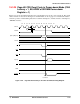
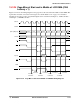
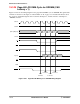
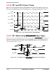
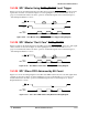
19.3.31 SPI 1 Slave FIFO Advanced by SS Rising Edge
Figure 19-32 shows the timing diagram for the SPI 1 slave FIFO advanced by SS rising edge. The signal
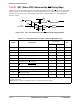
values and units of measure for Figure 19-27 through Figure 19-32 are found in Table 19-17. Detailed
information about the operation of individual signals can be found in Chapter 13, “Serial Peripheral
Interface 1 and 2.”
Figure 19-32. SPI 1 Slave FIFO Advanced by SS Rising Edge Timing Diagram
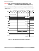
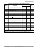
Table 19-17. Timing Parameters for Figure 19-27 Through Figure 19-32
Number Characteristic
(3.0 ± 0.3) V
Unit
Minimum Maximum
1 Clock edge to TxD data ready — 0.25T ns
2 RxD data ready to clock edge 0.25T — ns
3 Clock edge to RxD data hold time 0.25T — ns
4 DATA
_READY to SS output low — 2T ns
5SS
output low to first SCLK edge 2T — ns
6 Last SCLK edge to SS
output high T — ns
7SS
output high to DATA_READY low T — ns
8SS
output pulse width 2T + WAIT — ns
9SS
input low to first SCLK edge T — ns
10 SS
input pulse width 0 — ns
11 Pause between data word 0 — ns
Note:
T
= SPI clock period
WAIT = Number of sysclk or 32.768 KHz clocks per sample period control register
SS
(Input)
SCLK,
MOSI, MISO
9
11
10