
MC68VZ328 Integrated Processor User's Manual


19-24 MC68VZ328 User’s Manual
AC Electrical Characteristics
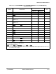
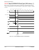
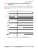
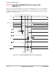
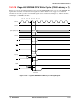
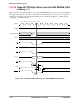
19.3.19 Page-Hit CPU Byte-Write Cycle for 8-Bit SDRAM (CAS
Latency = 1)
Figure 19-20 shows the timing diagram for the page-hit SDRAM CPU byte-write cycle for 8-bit SDRAM.
The signal values and units of measure for this figure are found in Table 19-16 on page 19-31. Detailed
information about the operation of individual signals can be found in both Chapter 8, “LCD Controller,”
and Chapter 7, “DRAM Controller.”
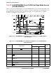
Figure 19-20. Page-Hit CPU Byte-Write Cycle for 8-Bit SDRAM Timing Diagram
S0 S2 S4 S6 S7S5S3S1
SDCLK
RAS
SCKEN
D[15:0]
CAS
A[16:1]/MD[15:0]
SDA10
CS
WE
DQM
DTACK
Write
Command
Col
Upper Byte Lower Byte
13
12