
MC68VZ328 Integrated Processor User's Manual


AC Electrical Characteristics
Electrical Characteristics 19-17
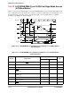
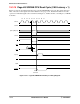
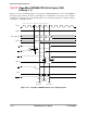
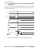
19.3.13 LCD Controller Timing
Figure 19-13 shows the LCD controller timing diagram for normal mode, and Figure 19-14 on page 19-18
displays the timing diagram for self-refresh mode. The signal values and units of measure for both figures
are found in Table 19-15 on page 19-18. Detailed information about the operation of individual signals can
be found in Chapter 8, “LCD Controller,” and Chapter 7, “DRAM Controller.”
Figure 19-13. LCD Controller Timing Diagram (Normal Mode)
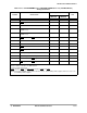
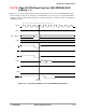
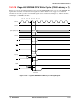
9 RASx pulse width (2N + 1)T —ns
10 CASx
pulse width (BC[1:0] = 00,01,10,11 in FPM) 28,58,88,118 — ns
11 CASx
precharge time 26 — ns
12 RASx
negated to CASx negated -28 — ns
13 Data-in hold after CASx
negated 0 — ns
14 OE
negated after CASx negated 0 2 ns
Note:
N is the number of words in one DMA transfer.
T is the system clock period.
RASx stands for RAS0 and RAS1. CASx stands for CAS0 and CAS1.
MSW is bit 5 and BC[1:0] comprises bits 13–12 in the DRAMC register. When the table identifies these bits, the
sequence of their listed values corresponds to the sequence of timing data provided.
Table 19-14. LCD DRAM DMA Cycle 16-Bit Fast Page Mode Access (LCD Bus Master)
Timing Parameters (Continued)
Number Characteristic
(3.0 ± 0.3) V
Unit
Minimum Maximum
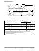
LFLM
LD[7:0]
LLP
LCLK
3 4
1
2