
MC68VZ328 Integrated Processor User's Manual


19-14 MC68VZ328 User’s Manual
AC Electrical Characteristics
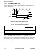
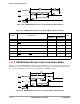
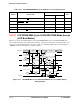
19.3.11 LCD DRAM DMA Cycle 16-Bit EDO RAM Mode Access
(LCD Bus Master)
Figure 19-11 shows the timing diagram for the LCD DRAM DMA cycle for 16-bit EDO RAM mode
access (LCD bus master). The signal values and units of measure for this figure are found in Table 19-13
on page 19-15. Detailed information about the operation of individual signals can be found in Chapter 7,
“DRAM Controller,” and Chapter 8, “LCD Controller.”
Figure 19-11. LCD DRAM DMA Cycle 16-Bit EDO RAM Mode Access (LCD Bus Master)
Timing Diagram
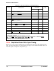
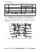
Table 19-12. LCD SRAM/ROM DMA Cycle 16-Bit Mode Access Timing Parameters
Number Characteristic
(3.0 ± 0.3) V
Unit
Minimum Maximum
1 Address valid to CSx
asserted 20 —ns
2UWE
/LWE to CSx asserted 28 — ns
3 Data setup time 16 — ns
4 CLKO to address valid — 10 ns
5 CLKO high to CSx
—10ns
MD[12:0]
CASx
RASx
DWE
OE
D[15:0]
4
1
8
9
5
2
6
11
10 12
14
7 133
Row Col 1 Col 2 Col 3
7