
MC68VZ328 Integrated Processor User's Manual


AC Electrical Characteristics
Electrical Characteristics 19-13
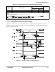
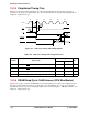
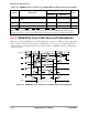
19.3.10 LCD SRAM/ROM DMA Cycle 16-Bit Mode Access (1
Wait State)
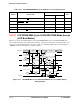
Figure 19-10 shows the LCD SRAM/ROM DMA cycle timing diagram for 16-bit access (1 wait state).
Note that WS is the number of wait states in the current memory access cycle. The signal values and units
of measure for this figure are found in Table 19-12 on page 19-14. Detailed information about the
operation of individual signals can be found in Chapter 7, “DRAM Controller,” and Chapter 8, “LCD
Controller.”
Figure 19-10. LCD SRAM/ROM DMA Cycle 16-Bit Mode Access Timing Diagram
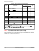
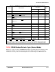
Table 19-11. DRAM Hidden Refresh Cycle (Low-Power Mode) Timing Parameters
Number Characteristic
(3.0 ± 0.3) V
Unit
Minimum Maximum
1 CASx
pulse width 120 —ns
2 RASx
pulse width 120 — ns
3 CASx
asserted to RASx asserted 30 — ns
4 CASx
negated to RASx negated 30 — ns
5 Refresh cycle (using 32.768 KHz crystal) 15 — us
5 Refresh cycle (using 38.400 KHz crystal) 13 — us
6DWE
negated before CASx asserted 58 — ns
Note: R
ASx stands for RAS0 and RAS1. CASx stands for CAS0 and CAS1.
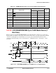
5
CLKO
CSx
A[31:0]
UWE
/LWE
OE
D[15:0]
2+1WS 2+1WS 2+1WS
4
1
3
2
Addr
Addr+2Addr+1 Addr+n