
MC68VZ328 Integrated Processor User's Manual


19-12 MC68VZ328 User’s Manual
AC Electrical Characteristics
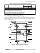
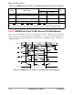
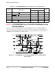
Figure 19-8. DRAM Hidden Refresh Cycle (Normal Mode) Timing Diagram
19.3.9 DRAM Hidden Refresh Cycle (Low-Power Mode)
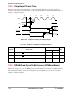
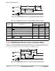
Figure 19-9 shows the DRAM hidden refresh cycle timing diagram for low-power mode. The signal values
and units of measure for this figure are found in Table 19-11 on page 19-13. Detailed information about
the operation of individual signals can be found in Chapter 7, “DRAM Controller.”
Figure 19-9. DRAM Hidden Refresh Cycle (Low-Power Mode) Timing Diagram
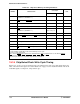
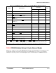
Table 19-10. DRAM Hidden Refresh Cycle (Normal Mode) Timing Parameters
Number Characteristic
(3.0 ± 0.3) V
Unit
Minimum Maximum
1 CASx
pulse width 88 —ns
2 RASx
pulse width 88 — ns
3 CASx
asserted to RASx asserted 28 32 ns
4 RASx
negated to CASx negated -28 — ns
5 CASx
negated to next CASx asserted 88 — ns
6DWE
negated before CASx asserted 58 — ns
Note: R
ASx stands for RAS0 and RAS1. CASx stands for CAS0 and CAS1.
CASx
DWE
RASx
51
23
6
4
CASx
DWE
RASx
1
5
3 4
6 2