
MC68VZ328 Integrated Processor User's Manual


AC Electrical Characteristics
Electrical Characteristics 19-11
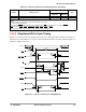
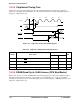
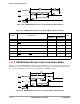
19.3.8 DRAM Hidden Refresh Cycle (Normal Mode)
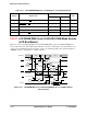
Figure 19-8 on page 19-12 shows the DRAM hidden refresh cycle timing diagram for normal mode. The
signal values and units of measure for this figure are found in Table 19-10 on page 19-12. Detailed
information about the operation of individual signals can be found in Chapter 7, “DRAM Controller.”
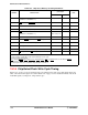
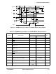
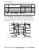
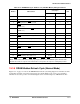
Table 19-9. DRAM Write Cycle 16-Bit Access (CPU Bus Master) Timing Parameters
Number Characteristic
(3.0 ± 0.3) V
Unit
Minimum Maximum
1 Row address valid to RASx
asserted 40 —ns
2DWE
asserted before CASx asserted 25 — ns
3OE
negated before RASx asserted 0 — ns
4 RASx
asserted before row address invalid
(MSW = 0,1)
12,27 — ns
5 Column address valid to CASx
asserted
(MSW = 0,1)
10,25 — ns
6 RASx asserted to CASx asserted (MSW = 0,1) 28,58 — ns
7 RASx
pulse width (SLW = 0,1) 90,120 — ns
8 CASx
pulse width (BC[1:0] = 00,01,10,11) 28,58,88,118 — ns
9 Data-out valid before CASx
asserted 25 — ns
10 Data-out hold after CASx
negated 25 — ns
11 DWE
negated after CASx negated 0 — ns
12 CASx
asserted before column address invalid 50 — ns
13 RASx
negated after CASx negated 28 — ns
14 RASx
precharge time (SLW = 0,1) 50,118 — ns
Note: RASx
stands for RAS0 and RAS1. CASx stands for CAS0 and CAS1.
Note: MSW is bit 5, SLW is bit 3, and BC[1:0] comprises bits 13–12 in the DRAMC register. When the table
identifies these bits, the sequence of their listed values corresponds to the sequence of timing data provided.