
MC68VZ328 Integrated Processor User's Manual


AC Electrical Characteristics
Electrical Characteristics 19-7
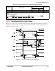
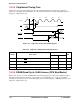
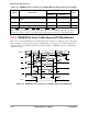
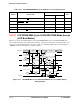
Figure 19-4. Chip-Select Flash Write Cycle Timing Diagram
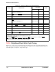
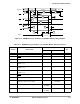
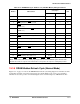
Table 19-6. Chip-Select Flash Write Cycle Timing Parameters
Number Characteristic
(3.0 ± 0.3) V
Unit
Minimum Maximum
1 Address valid to CSx
asserted
(bit ECDS = 0, bit ECDS = 1)
20, 20 - T/2 —ns
2CSx
asserted to UWE/LWE asserted 20 40 ns
3CSx
asserted to data-out valid — 30 ns
4 External DTACK
input setup from CSx asserted — 20 + nT ns
5CSx
pulse width
(bit ECDS = 0, bit ECDS = 1)
60 + nT,
(60 + T/2) + nT
—ns
6UWE/LWE negated before CSx is negated 10 20 ns
7 External DTACK
input hold after CSx is negated 0 — ns
8 Data-out hold after CSx
is negated 8 — ns
9CSx
negated to data-out in Hi-Z — 18 ns
Note:
n is the number of wait states in the current memory access cycle.
T is the system clock period.
The external DTACK input requirement is eliminated when CSx is programmed to use the internal DTACK.
CSx
stands for CSA0, CSA1, CSB0, CSB1, CSC0, CSC1, CSD0, or CSD1.
A value in parentheses is used when early detection is turned on.
A[31:0]
CSx
UWE/LWE
OE
D[15:0]
DTACK
51
2 6
3
9
8
4 7