
MC68VZ328 Integrated Processor User's Manual

19-4 MC68VZ328 User’s Manual
AC Electrical Characteristics
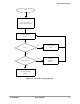
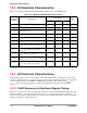
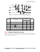
Figure 19-2. Chip-Select Read Cycle Timing Diagram
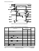
Table 19-4. Chip-Select Read Cycle Timing Parameters
Number Characteristic
(3.0 ± 0.3) V
Unit
Minimum Maximum
1 Address valid to CSx
asserted
(bit ECDS = 0, bit ECDS = 1)
20, 20 - T/2 —ns
2UWE/LWE negated before row address valid 0 — ns
3CSx
asserted to OE asserted — 0 ns
4 Data-in valid from CSx
asserted — 35 + nT ns
5 External DTACK
input setup from CSx asserted — 20 + nT ns
6CSx
pulse width
(bit ECDS = 0, bit ECDS = 1)
60 + nT,
(60 + T/2) + nT
—ns
7 External DTACK
input hold after CSx is negated 0 — ns
8 Data-in hold after CSx
is negated 0 — ns
9OE
negated after CSx is negated 0 10 ns
10 UB/LB
asserted to CSx asserted (16-bit SRAM) 10 — ns
A[31:0]
CSx
UWE/LWE
OE
D[15:0]
DTACK
UDS/LDS
UB/LB
1 6
2
3 9
4
5
8
7
1110