
MC68VZ328 Integrated Processor User's Manual

13-4 MC68VZ328 User’s Manual
SPI 1 Programming Model
13.3 SPI 1 Programming Model
This section provides information for programming SPI 1.
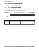
13.3.1 SPI 1 Receive Data Register
This read-only register holds the top of the 8 × 16 RxFIFO, which receives data from an external SPI
device during data transaction. The bit position assignments for this register are shown in the following
register display. The settings for this register are described in Table 13-1.
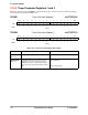
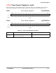
SPIRXD SPI 1 Receive Data Register 0x(FF)FFF700
BIT 7 6 5 4 3 2 1 BIT 0
DATA
TYPE r r r r r r r r
RESET
0 0 0 0 0 0 0 0
0x0000
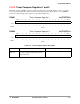
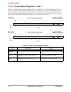
Table 13-1. SPI 1 Receive Data Register Description
Name Description Setting
DATA
Bits 7–0
Data—Top of SPI 1’s RxFIFO (8 × 16) The data in this register has no meaning if the RR bit
in the interrupt control/status register is cleared.