
MC68VZ328 Integrated Processor User's Manual

Programming Model
I/O Ports 10-33
Bits 0–3 are control signals connected to SPI 1. Their operation is detailed in Section 13.2.4, “SPI 1
Signals,” on page 13-3. The remaining 4 bits are control signals for UART 2; more information appears in
Section 14.2.3, “Serial Interface Signals,” on page 14-3.
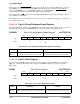
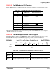
10.4.9.4 Port J Pull-up Enable Register
The pull-up enable register (PJPUEN) controls the pull-up resistors for each line in Port J. The bit settings
for the PJPUEN register are shown in Table 10-44.
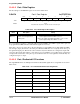
PJPUEN Port J Pull-up Enable Register 0x(FF)FFF43A
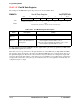
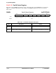
10.4.9.5 Port J Select Register
The select register (PJSEL) determines if a bit position in the data register (PJDATA) is assigned as a
GPIO or to a dedicated I/O function. The bit settings for the PJSEL register are shown in Table 10-45.
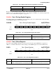
PJSEL Port J Select Register 0x(FF)FFF43B
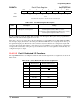
7 Data bit 7 CTS2
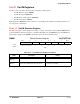
BIT 7654321BIT 0
PU7PU6PU5PU4PU3PU2PU1PU0
TYPE rw rw rw rw rw rw rw rw
RESET
11111111
0xFF
Table 10-44. Port J Pull-up Enable Register Description
Name Description Setting
PUx
Bits 7–0
Pull-up—These bits enable the pull-up resis-
tors on the port
0 = Pull-up resistors are disabled
1 = Pull-up resistors are enabled
BIT 7654321BIT 0
SEL7 SEL6 SEL5 SEL4 SEL3 SEL2 SEL1 SEL0
TYPE rw rw rw rw rw rw rw rw
RESET
11101111
0xEF
Table 10-45. Port J Select Register Description
Name Description Setting
SELx
Bits 7–0
Select—These bits select whether the internal chip
function or I/O port signals are connected to the pins.
0 = The dedicated function pins are connected.
1 = The I/O port function pins are connected.
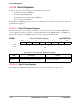
Table 10-43. Port J Dedicated I/O Function Assignments (Continued)
Bit GPIO Function Dedicated I/O Function