
MC68VZ328 Integrated Processor User's Manual


Programming Model
LCD Controller 8-19
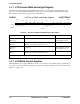
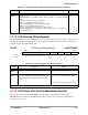
8.3.15 LCD Panning Offset Register
The LCD panning offset register (LPOSR) is used to control how many pixels the picture is shifted to the
left
. The bit assignments for the register are shown in the following register display. The settings for the
bits in the register are listed in Table 8-16.
LPOSR LCD Panning Offset Register 0x(FF)FFFA2D
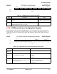
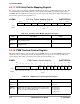
8.3.16 LCD Frame Rate Control Modulation Register
This register of address space 0x(FF)FFFA31 is used for frame rate modulation control in the
MC68EZ328, but it is unused in the MC68VZ328. This register is removed and not available for the
temporary storage of data.
RRAx
Bits 9–0
Refresh Rate 9–0—These bits contain the frame period, which can be calculated as
follows:
FRAME PERIOD = (12 + XMAX + RRA) x YMAX x (PXCD + 1) x LCDCLK_PERIOD
where:
Frame period = time for each screen update
XMAX = screen width in number of pixels
RRA = hexadecimal value stored in the LRRA register
YMAX = screen height in number of pixels
PXCD = hexadecimal value stored in the LPXCD register
LCDCLK_PERIOD: refer to Section 4.4.1, “PLL Control Register,” on page 4-8 for
setting LCDCLK period
See descrip-
tion.
BIT 7654321BIT 0
POS3 POS2 POS1 POS0
TYPE
rw rw rw rw
RESET
00000000
0x00
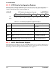
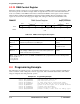
Table 8-16. LCD Panning Offset Register Description
Name Description Setting
Reserved
Bits 7
–4
Reserved These bits are reserved and should be set to
0.
POSx
Bits 3–0
Pixel Offset Code—These bits specify the number
of pixels being shifted to the left of the display panel.
This is independent of the black-and-white or gray
mode.
0001 = Picture is shifted 1 pixel to the left.
0010 = Picture is shifted 2 pixels to the left.
.
.
.
1111 = Picture is shifted 15 pixels to the left.
Note: When the LOPSR register is being modified, the software must adjust the cursor’s reference position.
Table 8-15. LCD Refresh Rate Adjustment Register Description (Continued)
Name Description Setting