
MC68VZ328 Integrated Processor User's Manual


Programming Model
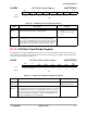
LCD Controller 8-17
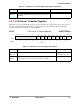
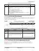
LACDRC LACD Rate Control Register 0x(FF)FFFA23
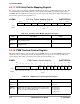
8.3.12 LCD Pixel Clock Divider Register
The LCD pixel clock divider (LPXCD) register is used to program the divider, which generates the pixel
clock. The bit assignments for the register are shown in the following register display. The settings for the
bits in the register are listed in Table 8-13.
LPXCD LCD Pixel Clock Divider Register 0x(FF)FFFA25
BIT 7654321BIT 0
ACDSLT ACD6 ACD5 ACD4 ACD3 ACD2 ACD1 ACD0
TYPE rw rw rw rw rw rw rw rw
RESET
00000000
0x00
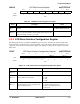
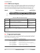
Table 8-12. LACD Rate Control Register Description
Name Description Setting
ACDSLT
Bit 7
Clock Source Select—This bit selects the clock source for the
internal counter that generates an LACD signal.
0 = Select frame pulse as input
clock
1 = Select line pulse as input
clock
ACDx
Bits 6–0
Alternate Crystal Direction Control 6–0—These bits represent
the ACD toggle rate control code. The LACD signal will toggle
once every 1 to 128 FLM/LP cycles based on the value specified
in this register. The actual number of FLM cycles is the value pro-
grammed plus one. Shorter cycles tend to give better results.
See description
BIT 7654321BIT 0
PCD5 PCD4 PCD3 PCD2 PCD1 PCD0
TYPE
rw rw rw rw rw rw
RESET
00000000
0x00
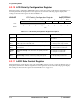
Table 8-13. LCD Pixel Clock Divider Register Description
Name Description Setting
Reserved
Bits 7–6
Reserved These bits are reserved
and should be set to 0.
PCDx
Bits 5–0
Pixel Clock Divider 5–0—These bits represent the pixel clock divisor.
The LCDCLK signal from the PLL is divided by N (PCD5–0 + 1) to yield
the actual pixel clock. Values of 1–63 will yield N = 2 to N = 64. If these
bits are set to 0 (N = 1), the PIX clock will be used directly, bypassing
the divider circuit. Refer to Chapter 4, “Clock Generation Module and
Power Control Module,” for more information.
See description.