
MC68VZ328 Integrated Processor User's Manual


6-20 MC68VZ328 User’s Manual
Programming Model
6.3.7 Chip-Select Control Register 3
This register controls minor timing trims for static memory access.
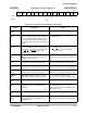
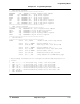
CSCTRL3 Chip-Select Control Register 3 0x(FF)FFF150
Example 6-2 on page 6-21 demonstrates how to initialize the chip-select with a particular memory
configuration.
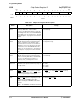
BIT 15 14 13 12 11 10 987654321BIT 0
EWE WPEXT LCWS AST DST CST
TYPE rw rw rw rw rw rw
RESET
1 0 0 1 1 1 000000000 0
0x9C00
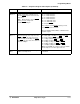
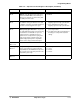
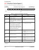
Table 6-14. Chip-Select Control Register 3 Description
Name Description Setting
EWE
Bit 15
End Write Early—When this bit is set, the
RAM write-enable signal negates before the
CS signal is negated.
0 = Disabled.
1 = Enabled.
WPEXT
Bit 14
Write Pulse to CS Negation Margin
Extension—When EWE is set, WPEXT is set
to extend the WE negation to CS negation by
one more clock.
0 = Disabled.
1 = Enabled.
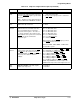
LCWS
Bit 13
Wait State Trim for LCD-SRAM
Access—When this bit is set, one additional
wait state is added to the LCD-SRAM access
cycle. For example, if the wait state is set to
zero, all CPU accesses require 4 cycles to
complete, the chip-select signal to SRAM lasts
2.5 CPU clock cycles, and 2 cycles are used
for LCD access. When LCWS is enabled, the
LCD access is delayed; the access is
increased from 2 to 3 clock cycles.
0 = No additional wait state added.
1 = One additional wait state added.
AST
Bit 12
AS Toggle Enable—Enables AS toggling
between two 8-bit transfers.
0 = Disable AS toggling between two 8-bit
transfers.
1 = Enable AS toggling between two 8-bit
transfers.
DST
Bit 11
DS Toggle Enable—Enables DS toggling
between two 8-bit transfers.
0 = Disable DS toggling between two 8-bit
transfers.
1 = Enable DS toggling between two 8-bit
transfers.
CST
Bit 10
CS Toggle Enable—Enables CS toggling
between two 8-bit transfers.
0 = Disable CS toggling between two 8-bit
transfers.
1 = Enable CS toggling between two 8-bit
transfers.
Reserved
Bits 9
–0
Reserved These bits are reserved and should be set to
0.