
MC68VZ328 Integrated Processor User's Manual

Programming Model
Chip-Select Logic 6-15
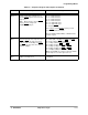
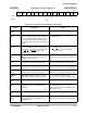
FLASH
Bit 8
Flash Memory Support—When enabled,
this bit provides support for flash memory by
forcing the LWE/UWE signal to go active after
chip-select.
Note: This bit is used for expanded memory
size for CSD when the DRAM bit is enabled.
0 = The chip-select and LWE
/UWE signals go active
at the same clock edge.
1 = The chip-select signal goes low 1 clock before
LWE
/UWE.
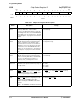
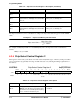
BSW
Bit 7
Data Bus Width—This bit sets the data bus
width for this chip-select area.
0 = 8 bit.
1 = 16 bit.
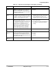
WS3–1
Bits 6–4
Wait State—This field contains the 3 most
significant bits of the 4-bit wait-state value.
The least significant bit is located in the
chip-select control register 1. The value of
these 4 bits determines the number of wait
states added to a bus cycle before an internal
DTACK
is asserted to terminate the
chip-select cycle.
000 = 0 + WS0 wait states.
001 = 2 + WS0 wait states.
010 = 4 + WS0 wait states.
011 = 6 + WS0 wait states.
100 = 8 + WS0 wait states.
101 = 10 + WS0 wait states.
110 = 12 + WS0 wait states.
111 = External DTACK.
When using the external DTACK signal, you must
select DTACK
function in Port G.
WS0 is the DWS0, CWS0, BWS0, or AWS0 bit in
the CSCTRL1 register.
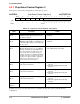
SIZ
Bits 3–1
Chip-Select Size—This field determines the
memory range of the chip-select. For CSAx
and CSBx
, the chip-select size is between
128K and 16 Mbyte. For CSCx
and CSDx, the
chip-select size is between 32K and
16 Mbyte.
000 = 128K (32K or 8 Mbyte* for CSCx
and CSDx).
001 = 256K (64K or 16 Mbyte* for CSCx
and CSDx).
010 = 512K (128K for CSCx
and CSDx).
011 = 1 Mbyte (256K for CSCx
and CSDx).
100 = 2 Mbyte (512K for CSCx
and CSDx).
101 = 4 Mbyte (1 Mbyte for CSCx
and CSDx).
110 = 8 Mbyte (2 Mbyte for CSCx
and CSDx).
111 = 16 Mbyte (4 Mbyte for CSCx
and CSDx).
* Note: Large DRAM size selection requires the
DSIZ3 bit in the chip-select control register to be set.
EN
Bit 0
Chip-Select Enable—This write-only bit
enables each chip-select.
0 = Disabled.
1 = Enabled.
Table 6-10. Chip-Select Register D Description (Continued)
Name Description Setting