
Computer Hardware User Manual


Carrier Modulator Transmitter (CMT)
Overview
MC68HC05RC16 — Rev. 3.0 General Release Specification
MOTOROLA Carrier Modulator Transmitter (CMT) 69
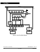
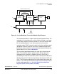
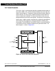
Figure 9-1. Carrier Modulator Transmitter Module Block Diagram
The modulator provides a simple method to control protocol timing. The
modulator has a resolution of 4 µs with a 2-MHz oscillator. It can count
system clocks to provide real-time control or it can count carrier clocks
for self-clocked protocols. It can either gate the carrier onto the
modulator output (TIME), control the logic level of the modulator output
(baseband) or directly route the carrier to the modulator output while
providing a signal to switch the carrier generator between high/low time
register buffers (FSK). See 9.5 Modulator.
The transmitter output block controls the state of the infrared out pin
(IRO). The modulator output is gated on to the IRO pin when the
modulator/carrier generator is enabled. Otherwise, the IRO pin is
controlled by the state of the IRO latch, which is directly accessible to the
CPU by means of bit 7 of the carrier generator data registers CHR1 and
CLR1. The IRO latch can be written to on either edge of the internal bus
clock (f
osc
/2), allowing for IR waveforms which have a resolution of twice
the bus clock frequency (f
osc
). See 9.4.2 Carrier Generator Data
Registers (CHR1, CLR1, CHR2, and CLR2).
f
OSC
CARRIER
GENERATOR
MODULATOR
CARRIER
OUT
MODULATOR
OUT
MODULATOR/
TRANSMITTER
OUTPUT
BASE
MODE
PRIMARY/SECONDARY SELECT
CPU INTERFACE
IRO
PIN
EOC FLAG
f
OSC
÷ 2
DB AB EOC INTERRUPT
EOC
ENABLE
.
INTERRUPT
CARRIER
ENABLE