
Specifications


5
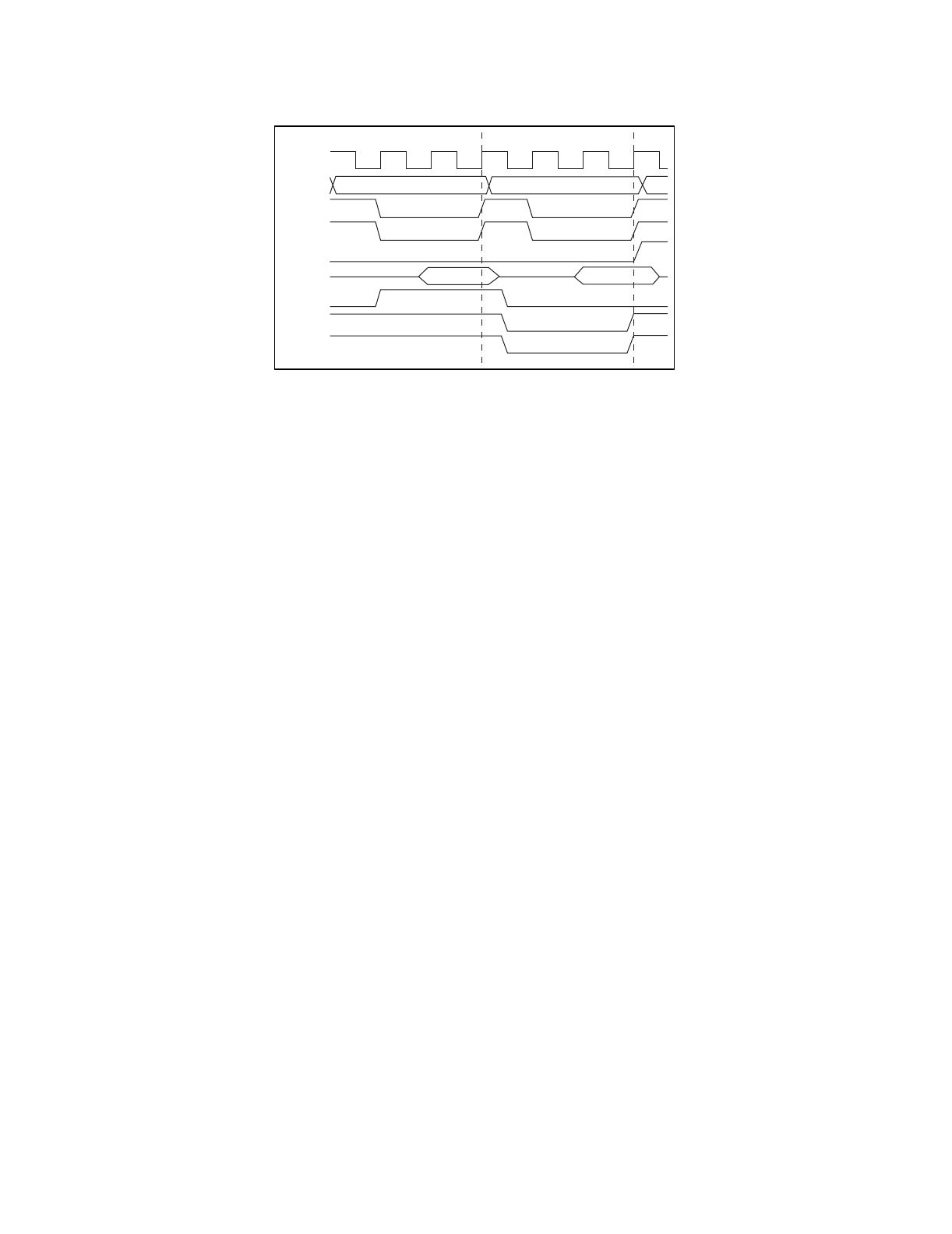
Figure 5. DMA Write (TNT4882 to Memory) Timing Diagram
Asynchronous Bus Operation
Normally, the TNT4882 is used in one chip mode. See Chapter 2 in the TNT4882 Programmer Reference Manual. To
maintain backwards compatibility, the TNT4882 can be used in two chip mode. In the two chip mode, the TNT4882
duplicates the Turbo488/NAT4882 chipset. In two chip mode the processor can access registers in both the Turbo488
and NAT4882 but all NAT4882 accesses have to pass through the Turbo488, hence they take a little longer time. To
accommodate for this feature, one can use the asynchronous timing of MC68340 processor. Asynchronous timing on
MC68340 can be controlled by using the DSACKNx pins. The TNT4882 provides two signals namely RDY1 and
CPUACC which can allow the user to handle delays in I/O accesses.
The TNT4882 asserts CPUACC to indicate the processor to lengthen the current I/O access. RDY1 indicates that the
TNT4882 is ready for the host interface to complete the lengthened cycle if CPUACC is asserted. If CPUACC is not
asserted, RDY1 indicates that the current I/O cycle does not need to be lengthened, it does not indicate that the current
cycle has finished. Therefore, DSACKN1 should be negated when CPUACC is asserted and RDY1 is negated. See
Chapter 5 in the TNT4882 Programmer Reference Manual.
S0 S1 S2 S3 S4 S5 S0 S1 S2 S3 S4 S5 S0
CPU Cycle DMA Cycle
DACKN
CLK
ADDR
ASN
DSN
R/W
DATA
DRQ
(TNT)
RDN