
Specifications


4
TNT4882 RDN, WRN Signals
During write accesses, the TNT4882 latches data on the rising edge of WRN. The TNT4882 drives its data buses when
RDN is asserted during read accesses. The processor asserts DSN to indicate that an external device should place valid
data on the bus during a read access, and that valid data is on the data bus during a write access. The R/W signal
indicates the direction of data transfer on the bus. When Direct Memory Access (DMA) is used, DACKN is asserted
by the CPU to indicate that a word is being transferred. Since we are implementing single address DMA, DACKN and
R/W signals should be used to control RDN and WRN during DMA accesses. Table 2 shows the RDN and WRN
signals with respect to R/W, DSN, DACKN.
Table 2.
RDN and WRN Signals of TNT4882
TNT4882 DMA Signals
The processor has a built-in DMA controller so our system does not require an external DMA controller. The system
supports 16-bit Single Address DMA transfers between system memory and the TNT4882 FIFOs. Only one DMA
channel is used. Since MC68340 will start DMA when DREQN1 is asserted, the DRQ signal of the TNT4882 must be
inverted and then connected to the DREQN1 pin of MC68340. The DACKN signal from the TNT4882 can be
connected directly to the DACKN1 pin of MC68340. Figures 4 and 5 show the DMA read and write cycles
respectively.
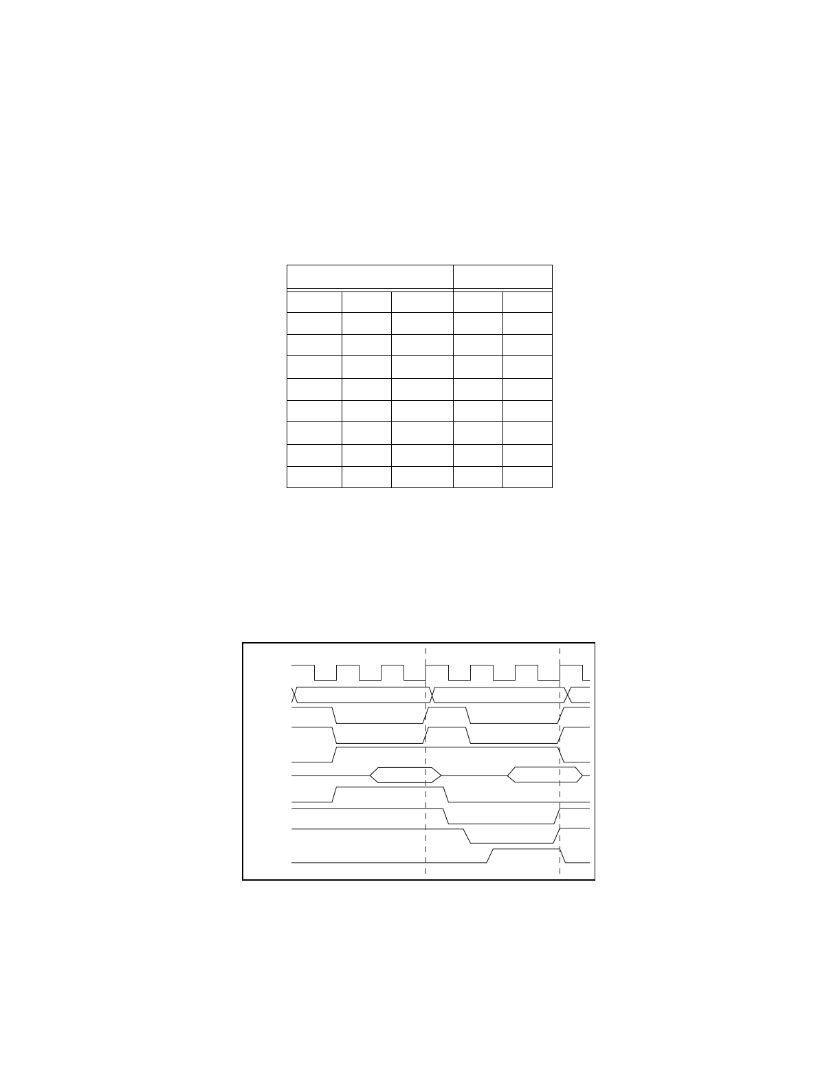
Figure 4.
DMA Read (Memory to TNT4882) Timing Diagram
MC68340 TNT4882
R/W DSN DACKN RDN WRN
0 0 0 0 1
0 0 1 1 0
0 1 0 0 1
0 1 1 1 1
1 0 0 1 0
1 0 1 0 1
1 1 0 1 0
1 1 1 1 1
CPU Cycle
S0 S1 S2 S3 S4 S5 S0 S1 S2 S3 S4 S5 S0
DACKN
DMA Cycle
CLK
ADDR
ASN
DSN
R/W
DATA
DRQ
(TNT)
WRN
RDY1