
Specifications


3
TNT4882 ABUSN, BBUSN Signals
The TNT4882 has the capability of using either of its data busses for 8-bit I/O accesses. Either Bus A (D15-8) or Bus
B (D7-0) can be selected using the ABUSN and BBUSN signals. These two signals can be controlled by using SIZ0
and A0 signals of the processor. Whenever accesses are made to an odd byte address, the processor uses the lower byte
of the data bus and whenever accesses are made to an even byte address, the processor uses the upper byte of the data
bus. Table 1 shows the ABUSN and BBUSN signals with respect to SIZ0 and A0.
Table 1.
ABUSN and BBUSN Signal of TNT4882
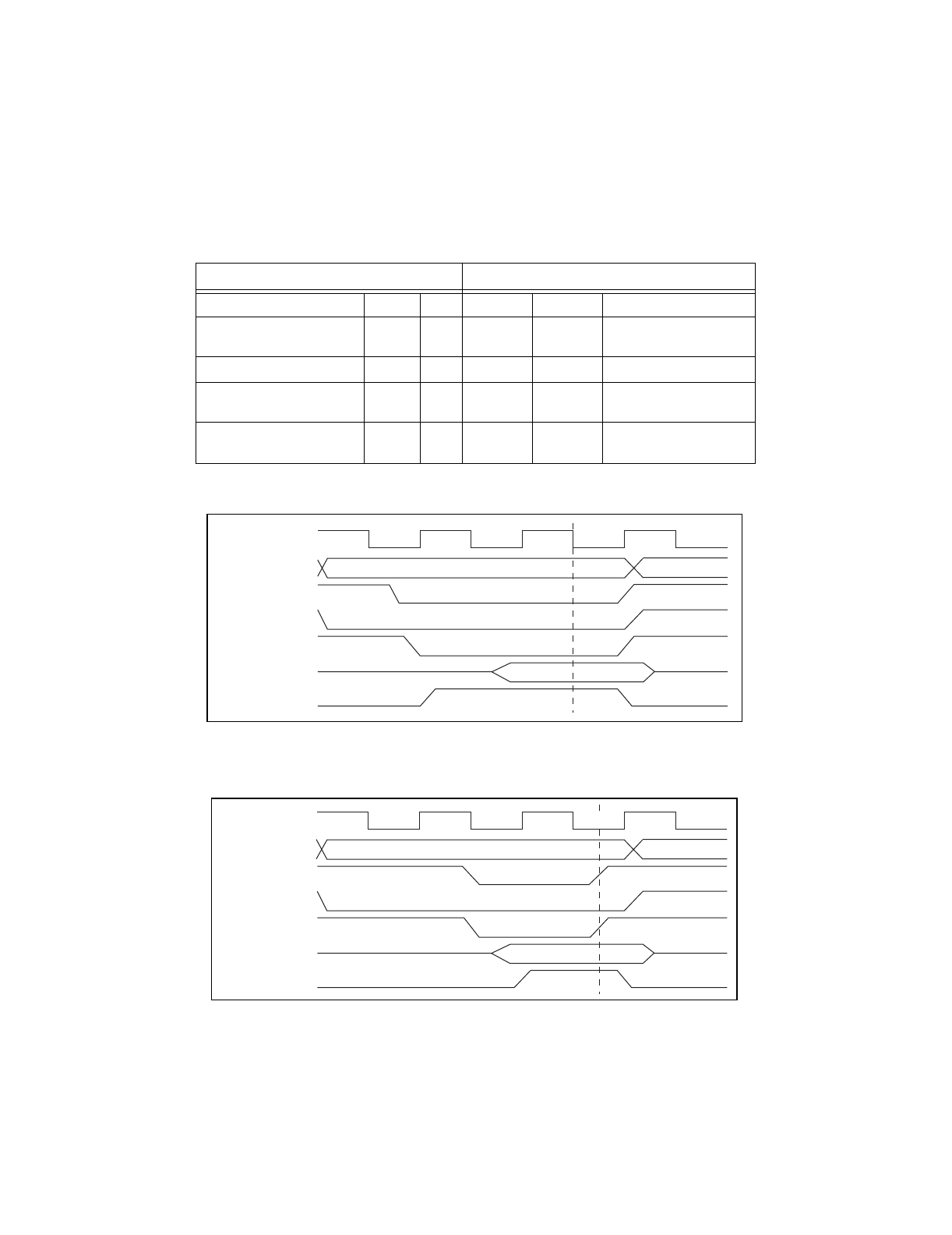
Figures 2 and 3 show the CPU read and write timing diagrams, respectively.
Figure 2.
CPU Read Timing Diagram
Figure 3.
CPU Write Timing Diagram
MC68340 TNT4882
Transfer Case SIZ0 A0 ABUSN BBUSN Type of Access
Word Access OR Longword
Access
0 0 0 0 16-bit Access
Not Used 0 1 X X NONE
Even Byte Access 1 0 0 1 8-bit Access on Upper Byte
Lane
Odd Byte Access 1 1 1 0 8-bit Access on Lower Byte
Lane
S5S0 S1 S2 S3 S4 S0
CLK
ADDR R/W
DSN
TNT4882 CSN
TNT4882 DATA
TNT4882 RDY1
TNT4882 RDN
S5S0 S1 S2 S3 S4 S0
CLK
ADDR R/W
DSN
TNT4882 CSN
DATA
TNT4882 RDY1
TNT4882 WRN