
user manual
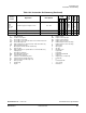


Electrical Specifications
General Release Specification MC68HC05RC16 — Rev. 3.0
106 Electrical Specifications MOTOROLA
11.6 DC Electrical Characteristics (5.0 Vdc)
Characteristic Symbol Min Typ Max Unit
Output Voltage
I
LOAD
= 10.0 µA
I
LOAD
= –10.0 µA
V
OL
V
OH
—
V
DD
– 0.1
—
—
0.1
—
V
Output High Voltage
(I
LOAD
–2.0 mA) Port A, Port B, Port C (1–7)
(I
LOAD
–20 mA) IRO
(I
LOAD
–4.0 mA) Port C (Bit 0)
V
OH
V
DD
–0.8
V
DD
–0.8
V
DD
–0.8
V
DD
–0.2
V
DD
–0.2
V
DD
–0.2
—
—
—
V
Output Low Voltage
(I
LOAD
= 3.0 mA) Port A, Port B, Port C (1–7)
(I
LOAD
= 25.0 mA) IRO
(I
LOAD
= 20.0 mA) Port C (Bit 0)
V
OL
—
—
—
0.2
0.2
0.2
0.4
0.4
0.4
V
Input High Voltage
Port A, Port B, Port C, IRQ, RESET,
LPRST, OSC1
V
IH
0.7xV
DD
—V
DD
V
Input Low Voltage
Port A, Port B, Port C, IRQ, RESET,
LPRST, OSC1
V
IL
V
SS
— 0.2 x V
DD
V
Supply Current (see Notes)
Run
Wait
Stop
25
o
C
0 to +70
o
C
I
DD
—
—
—
—
2.3
0.5
0.3
0.3
4.0
1.0
10.0
20.0
mA
mA
µA
µA
I/O Ports Hi-Z Leakage Current
Port A, Port B, Port C
I
OZ
–10 — 10 µA
Input Current
RESET, LPRST, IRQ, OSC1
PB0–PB7 with Pullups Enabled
(V
IN
= 0.2 x V
DD
)
8
PB0–PB7 with Pullups Enabled
(V
IN
= 0.7 x V
DD
)
I
IN
–1
–100
–50
—
–330
–120
1
–700
–300
µA
Capacitance
Ports (as Input or Output)
RESET, LPRST, IRQ
C
OUT
C
INT
—
—
—
—
12
8
pF
NOTES:
1. V
DD
= 5.0 Vdc ± 10%, V
SS
= 0 Vdc, T
A
= 0 °C to +70 °C, unless otherwise noted
2. Typical values at midpoint of voltage range, 25 °C only, represent average measurements.
3. Wait I
DD
: only core timer active
4. Run (Operating) I
DD
, wait I
DD
: Measured using external square wave clock source (f
Osc
= 4.2 MHz); all inputs 0.2 V
from rail; no dc loads; less than 50 pF on all outputs; C
L
= 20 pF on OSC2
5. Wait, Stop I
DD
: Port A and port C configured as inputs, port B configured as outputs, V
IL
= 0.2 V, V
IH
= V
DD
–0.2 V
6. Stop I
DD
is measured with OSC1 = V
SS
.
7. Wait I
DD
is affected linearly by the OSC2 capacitance.
8. Pullups are designed to be capable of pulling to V
IH
within 1 µs for a 100 pF, 4-kΩ load.