
Development Board User's Manual


13
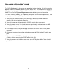
MCU_PORT
The MCU_PORT provides access to the peripheral features and I/O lines of the HC12 as
follows:
D0
1 2
D1
D2
3 4
D3
D4
5 6
D5
D6
7 8
D7
/XIRQ, PE0
9 10
/DBE, PE7
VFP
11 12
/LSTRB
PG6
13 14
PG7
PG4
15 16
PG5
PG2
17 18
PG3
PG0
19 20
PG1
PH6
21 22
PH7
PH4
23 24
PH5
PH2
25 26
PH3
PH0
27 28
PH1
PS0 / RXD0
29 30
PS1 / TXD0
PS2 / RXD1
31 32
PS3 / TXD1
PS4
33 34
PS5
PS6
35 36
PS7
PCAN6
37 38
PCAN7
PCAN4
39 40
PCAN5
PCAN2
41 42
PCAN3
PCAN0
43 44
PCAN1
PT0
45 46
PT1
PT2
47 48
PT3
PT4
49 50
PT5
PT6
51 52
PT7
PP6
53 54
PP7
PP4
55 56
PP5
PP2
57 58
PP3
PP0
59 60
PP1
D0 – D7 Low Byte of the Data Bus in Wide Expanded
Mode. Port B in Single Chip Mode.
/XIRQ XIRQ interrupt input .
VFP Programming voltage, 12v, when CONFIG switch
position 5 is on.
/LSTRB LSTRB (PE3) output indicates 8 bit bus access.
Should be enabled in software for bus use.
PP0 – PP7 Port P I/O or PWM port.
PT0 – PT7 Port T I/O or Timer port.
PS0 – PS7 Port S I/O or Serial Port lines.
PG0 – PG7 Port G I/O or Key wakeup pins.
PH0 – PH7 Port H I/O or Key wakeup pins.
Also used by the KEYPAD Port.
RXD / TXD Serial Port (SCI) receive and transmit pins.
PCAN0 – PCAN7 CAN I/O lines.
CAN_PORT
1
GND
2
CAN-H
3
CAN-L
4
+5V
The CAN_PORT connector provides an interface to the MSCAN12 on
the microcontroller. This port provides a CAN transceiver device. See
the schematic drawing and the MC68HC912D60 data sheet for
information on using this peripheral.
RxCAN1-3 can be added to supply CAN port bus terminations as required (see schematic).