
Technical information


Chapter 2: Hardware Interface Description
December 15, 2009 G30 - Module Hardware Description 27
The board to board pins related to I
2
C bus interface description is given in Table 2-7:
SIM Interface
The G30 incorporates a SIM interface, which conforms to the GSM 11.11 and GSM 11.12
standards, that are based on the ISO/IEC 7816 standard. These standards define the electrical,
signaling and protocol specifications of a GSM SIM card.
Both 1.8 V and 3 V SIM types are supported; activation and deactivation with automatic voltage
switch from 1.8 V to 3 V is implemented.
G30 is designed to support two SIM card options with the same SIM signals: External SIM card,
or an on board Embedded SIM (eSIM), depending on the G30 model.
Table 2-8 details the SIM interface signals.
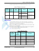
Table 2-7: I
2
C Interface Connections
Pin #
(81 pin LGA
interface)
Pin #
(70 pin
connector
interface)
G30
Signal Name
G30
I/O
Function Remarks
33 34 GPIO4/SCL O
I
2
C bus clock line I
2
C interface voltage
domain.
PU drain.
Value at reset: T/OD.
I/O GPIO
34 32 GPIO3/SDA I/O
I
2
C bus data line I
2
C interface voltage
domain.
PU drain.
Value at reset: T/OD.
I/O GPIO
Table 2-8: SIM Interface Signals
Pin #
(81 pin LGA
interface)
Pin #
(70 pin
connector
interface)
Signal Name Description
20 48 VSIM 2.85V/1.8V Supply to the SIM
21 44 SIM_RST Active low External SIM reset
signal
22 52 SIM_IO Serial input and output data
23 46 SIM_CLK Serial 3.25 MHz clock
59 50 SIM_PD_n Active low SIM card presence
detection
456eSIM_RESET Active low Embedded SIM reset
signal