
Technical information


Chapter 4: Mechanical Specifications
December 15, 2009 G30 - Module Hardware Description 79
Layout Recommendation
Note: This section applies to G30 LGA Model only.
Soldering Footprint
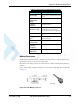
Figure 4-9 gives a layout recommendation for the G30.
Figure 4-9: G30 Soldering Footprint (Top View)
Note:
• Routing signals other then GND (Ground) within inner soldering footprint area of G30
(under G30) is not recommended.
• Vias inside pads are not recommended.
• Verify GND pads are well tied to ground plane layer by vias.