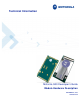
Technical Information Motorola G30 Developer’s Guide Module Hardware Description DECEMBER 15, 2009 6802986C55-A
SPECIFICATIONS SUBJECT TO CHANGE WITHOUT NOTICE Notice While reasonable efforts have been made to assure the accuracy of this document, Motorola, Inc. assumes no liability resulting from any inaccuracies or omissions in this document, or from use of the information obtained herein. The information in this document has been carefully checked and is believed to be entirely reliable. However, no responsibility is assumed for inaccuracies or omissions. Motorola, Inc.
Usage and Disclosure Restrictions License Agreements The software described in this document is the property of Motorola, Inc. and its licensors. It is furnished by express license agreement only and may be used only in accordance with the terms of such an agreement. Copyrighted Materials Software and documentation are copyrighted materials. Making unauthorized copies is prohibited by law.
This page intentionally left blank.
Table of Contents Manual Scope . . . . . . . . . . . . . . . . . . . . . . . . . . . . . . . . . . . . . . . . . . . . . . . . . . . . . . . . . . . . . . . . . . . .ix Target Audience . . . . . . . . . . . . . . . . . . . . . . . . . . . . . . . . . . . . . . . . . . . . . . . . . . . . . . . . . . . . . . . . . .ix Manual Organization . . . . . . . . . . . . . . . . . . . . . . . . . . . . . . . . . . . . . . . . . . . . . . . . . . . . . . . . . . . . . . .ix Applicable Documents . . . . . . . . . . . .
Table of Contents Turning the G30 Off . . . . . . . . . . . . . . . . . . . . . . . . . . . . . . . . . . . . . . . . . . . . . . . . . . . . . . . . . . . . 16 Turning the G30 Off Using PWR_ON . . . . . . . . . . . . . . . . . . . . . . . . . . . . . . . . . . . . . . . . . . . . 17 Power Loss shut down . . . . . . . . . . . . . . . . . . . . . . . . . . . . . . . . . . . . . . . . . . . . . . . . . . . . . . . . 17 Turning the G30 Off Using AT+MRST . . . . . . . . . . . . . . . . . . . . . . . . . . . .
Table of Contents Supply/power Pins . . . . . . . . . . . . . . . . . . . . . . . . . . . . . . . . . . . . . . . . . . . . . . . . . . . . . . . . . . . . . 52 Digital Pins . . . . . . . . . . . . . . . . . . . . . . . . . . . . . . . . . . . . . . . . . . . . . . . . . . . . . . . . . . . . . . . . . . . 52 Audio Pins . . . . . . . . . . . . . . . . . . . . . . . . . . . . . . . . . . . . . . . . . . . . . . . . . . . . . . . . . . . . . . . . . . . 56 ADC Pins . . . . . . . . . . . . . . . . . . . . . .
Table of Contents This page intentionally left blank.
List of Figures 2-1 2-2 2-3 2-4 2-5 2-6 2-7 2-8 2-9 2-10 2-11 2-12 2-13 2-14 2-15 2-16 2-17 2-18 2-19 2-20 2-21 2-22 2-23 3-1 3-2 4-1 4-2 4-3 4-4 4-5 4-6 4-7 4-8 4-9 G30 Block Diagram . . . . . . . . . . . . . . . . . . . . . . . . . . . . . . . . . . . . . . . . . . . . . . . . . . . . . . . . . . 9 Transmission Power Drops. . . . . . . . . . . . . . . . . . . . . . . . . . . . . . . . . . . . . . . . . . . . . . . . . . . . 13 Power Supply Turn-on . . . . . . . . . . . . . . . . . . . . . . . . . . . .
List of Tables 1-1 Product Specifications . . . . . . . . . . . . . . . . . . . . . . . . . . . . . . . . . . . . . . . . . . . . . . . . . . . . . . . . 2 2-1 2-2 2-3 2-4 2-5 2-6 2-7 2-8 2-9 2-10 2-11 2-12 2-13 2-14 2-15 2-16 2-17 2-18 2-19 2-20 2-21 2-22 3-1 3-2 3-3 3-4 3-5 3-6 3-7 3-8 3-9 3-10 3-11 3-12 3-13 G30 Operating Modes. . . . . . . . . . . . . . . . . . . . . . . . . . . . . . . . . . . . . . . . . . . . . . . . . . . . . . . . Power Supply Signals . . . . . . . . . . . . . . . . . . . . . .
Preface Manual Scope This manual provides the electrical, mechanical and environmental requirements for properly integrating the G30 module in a host application. This manual gives a complete set of hardware features and functions that may be provided by G30. The availability of any feature or function, which is described in this manual, depends on the hardware revision and software version of a specific G30 model. The parameters and values provided in this manual are defined under typical conditions.
Regulatory Requirements Regulatory Requirements The Federal Communications Commission (FCC) requires application for certification of digital devices in accordance with CFR Title 47, Part 2 and Part 15. This includes MPE calculation. As the G30 modem is not a standalone transceiver but is an integrated module, the G30 cannot be tested by itself for EME certification. It is, however, the integrator’s responsibility to have the completed device tested for EME certification.
Preface This equipment has been tested and found to comply with the limits for a Class B digital device, pursuant to part 15 of the FCC Rules. These limits are designed to provide reasonable protection against harmful interference in a residential installation. This equipment generates uses and can radiate radio frequency energy and, if not installed and used in accordance with the instructions, may cause harmful interference to radio communications.
Standards Antenna Installation • The antenna installation must provide a minimum separation distance of 20 cm from users and nearby persons and must not be co-located or operating in conjunction with any other antenna or transmitter. • Antenna installation should be done by a professional installer and should meet all FCC requirement as given in FCC part 15. • Combined cable loss and antenna gain • R&TTE requirements • 900 MHz GSM band: The combined cable loss and antenna gain must not exceed 4.
Preface GSM 03.40, Digital cellular telecommunication system (Phase 2+); Technical realization of the Short Message Service (SMS) Point-to-Point (PP), Version 5.3.0, July 1996, Reference TS/SMG-040340QR2. GSM 04.11 Digital cellular telecommunication system (Phase 2+); Point-to-Point (PP) Short Message Service (SMS) support on mobile radio interface, Version 5.1.0, March 1996, Reference TS/SMG-030411QR. GSM 03.
Text Conventions Warning Warning: Presents information to warn you of a potentially hazardous situation in which there is a possibility of personal injury. Important Important: Presents information to help you avoid an undesirable situation or provides additional information to help you understand a topic or concept. Caution Caution: xiv Presents information to identify a situation in which damage to software, stored data, or equipment could occur, thus avoiding the damage.
Preface Field Service For Field Service requests, use this email address: n2csfs01@motorola.com General Safety Remember!. . . safety depends on you! The following general safety precautions must be observed during all phases of operation, service, and repair of the equipment described in this manual. Failure to comply with these precautions or with specific warnings elsewhere in this manual violates safety standards of design, manufacture, and intended use of the equipment. Motorola, Inc.
Caring for the Environment • not replace components with power cable connected. Under certain conditions, dangerous voltages may exist even with the power cable removed • always disconnect power and discharge circuits before touching them Do not substitute parts or modify equipment Because of the danger of introducing additional hazards, do not install substitute parts or perform any unauthorized modification of equipment.
Preface Disposal of Motorola equipment in non-EU countries In non-EU countries, dispose of Motorola equipment in accordance with national and regional regulations.
How to Get Warranty Service? You must inform Motorola of the lack of conformity to the applicable specifications of any of the Products within a period of two (2) months from the date on which you detect a defect in material, workmanship or lack of conformity and in any event within a term not to exceed the Warranty Term, and must immediately submit the Product for service to Motorola's Authorized Repair or Service Center.
Preface In some cases, you may be requested to provide additional information concerning the maintenance of the Products by Motorola Authorized Service Centers only, therefore it is important to keep a record of any previous repairs, and make them available if questions arise concerning maintenance. Conditions This warranty will not apply if the type or serial numbers on the Product has been altered, deleted, duplicated, removed, or made illegible.
Installed Data 6. Defects or damage due to range, coverage, availability, grade of service, or operation of the cellular system by the cellular operator. 7. Defects or damage due to moist, liquid or spills of food. 8. Control unit coil cords in the Product that are stretched or have the modular tab broken. 9. All plastic surfaces and all other externally exposed parts that are scratched or damaged due to customer normal use.
Preface Revision History Manual Number 6802986C55-A Manual Title G30 - Module Hardware Description Version Information The following table lists the manual version, date of version, and remarks about the version.
Revision History This page intentionally left blank.
Chapter 1: Introduction The G30 is the newest member of Motorola's embedded cellular modules family. Designed with quad band GSM capabilities, which supports four GSM bands 850/900/1800/1900 MHz, and with GPRS multislot class 10, G30 can operate on any GSM/GPRS network to provide voice and data communications. The G30 is similar to a condensed cellular phone core, which can be integrated into any system or product that needs to transfer voice or data information over a cellular network.
Product Specifications Product Specifications Important: For safety regulations and requirements, see “Regulatory Requirements” on page x, “Regulatory Statement (Safety)” on page x and “Antenna and Transmission Safety Precautions” on page xi in “Preface” . Note: Motorola reserves the right to change the specifications without prior notice.
Table 1-1: Product Specifications (Cont.) Environmental Operational temperature: -30°C to +85°C Storage temperature: -40°C to +85°C Performance Operating voltage: 3.3 - 4.2 V Current consumption: In AT mode: < 1.
Product Specifications Table 1-1: Product Specifications (Cont.
Table 1-1: Product Specifications (Cont.
Regulatory and Approvals Regulatory and Approvals • • • • • • • R&TTE GCF FCC/CE PTCRB IC RoHS Anatel Brazil European Union Directives Conformance Statement Hereby, Motorola declares that this product is in compliance with • The essential requirements and other relevant provisions of Directive 1999/5/EC • All other relevant EU Directives IMEI: 350034/40/394721/9 0682 Type: G30 Product Approval Number The above gives an example of a typical Product Approval Number.
CFR 47 Part 15.21 Information to user The user's manual or instruction manual for an intentional or unintentional radiator shall caution the user that changes or modifications not expressly approved by the party responsible for compliance could void the user's authority to operate the equipment.
Regulatory and Approvals This page intentionally left blank.
Chapter 2: Hardware Interface Description The following paragraphs describe in details the hardware requirements for properly interfacing and operating the G30 module. Architecture Overview Figure 2-1 below illustrates the primary functional components of the G30.
Architecture Overview The G30 consists of the following blocks: Baseband The baseband IC is combined with the RF transceiver and the power management unit (PMU). This chipset provides all baseband and low power RF band functionality for GPRS/GSM, and includes: • Micro-controller Unit (MCU) for system and user code execution. • Digital Signal Processor (DSP) for voice and data processing. • Serial communications interfaces.
Chapter 2: Hardware Interface Description Operating Modes G30 incorporates several operating modes. Each operating mode is different in the active features and interfaces. Table 2-1 summarizes the general characteristics of the G30 operating modes and provides general guidelines for operation. Table 2-1: G30 Operating Modes Mode Description Features Not Powered VCC supply is disconnected. VRTC is disconnected. The G30 is Off. Any signals connected to the interface connector must be set tri-state.
Power Supply Power Supply The G30 power supply must be a single external DC voltage source of 3.3V to 4.2V. The power supply must be able to sustain the voltage level during a GSM transmit burst current surge, which may reach 2.0A. The G30 interface contacts for the main power supply, are described in Table 2-2. All these contacts must be used for proper operation.
Chapter 2: Hardware Interface Description Figure 2-2 illustrates the power supply behavior during GSM transmission. Figure 2-2: Transmission Power Drops Note: 1 TX slot is shown. It is recommended that the voltage drops during a transmit burst will not exceed 300mV, measured on the G30 interface connector. In any case, the G30 supply input must not drop below the minimum operating level during a transmit burst.
Power Supply Power Consumption Table 2-4 specifies typical G30 current consumption ratings in various operating modes. The current ratings refer to the overall G30 current consumption over the VCC supply. Table 2-4: G30 Current Ratings Parameter 14 Description Conditions Min Typ Max Unit IOFF RTC mode 90 µA IIDLE Idle mode 28 mA ISLEEP Low power mode 1.
Chapter 2: Hardware Interface Description Power On/Off Operation The G30 power on and off process includes two primary phases, which are indicated at the interface connector by the hardware input signal RESET_IN, and the output signal CTS. The RESET_IN is usually an input signal to the G30, and its main function is to initiate HW reset to the G30. However, this signal can also serve as "live indication" signal, and indicate whether G30 is powered on or off.
Power On/Off Operation Figure 2-3 illustrates the G30 power on upon application of a power supply. Figure 2-3: Power Supply Turn-on Turning the G30 On Using PWR_ON The PWR_ON input signal is set high by an internal pull-up resistor whenever a power supply is applied to G30. Therefore, it is recommended to operate this signal using an open collector/drain circuit connection. Asserting the PWR_ON signal low for a minimum of 600 milliseconds (0.6 seconds) and a maximum of 1.
Chapter 2: Hardware Interface Description Turning the G30 Off Using PWR_ON The PWR_ON signal is set high using an internal pull up resistor when power is applied to G30. Asserting the PWR_ON signal low for a minimum of 3 seconds will turn G30 off. This will initiate a normal power-off process, which includes disabling of all applications interfaces (UART, SIM card, audio, etc.) and closing the network connection. Figure 2-5 illustrates the power-off timings when using the PWR_ON signal.
Low Power Mode Low Power Mode The G30 incorporates an optional low power mode, called Sleep Mode, in which it operates in minimum functionality, and therefore draws significantly less current. During low power mode the G30 network connection is not lost. G30 continues to monitor the GSM network constantly for any incoming calls or data. During low power mode, all of the G30 interface signals are inactive and are kept in their previous state, prior to activating low power mode.
Chapter 2: Hardware Interface Description The G30 wakes up periodically from low power mode to page the GSM network for any incoming calls or data. After this short paging is completed, G30 returns to low power mode. During this short awake period, the serial interfaces are enabled and communications with the module is possible. The CTS signal is alternately enabled and disabled synchronously with the network paging cycle. CTS is enabled whenever G30 awakes to page the network.
Low Power Mode Temporary Termination of Low Power Mode Temporary termination of low power mode occurs when G30 switches from Sleep mode to Idle mode for a defined period, and then returns automatically to Sleep mode. Low power mode may be terminated temporarily by several sources, some of which are user initiated and others are initiated by the system. Using the WKUPI signal The WKUPI signal is an active low input, that is set high by default.
Chapter 2: Hardware Interface Description Data on the Serial interface While G30 is temporarily awake in Idle mode, data may be transmitted on the serial interface. In case data is being transmitted in any direction, G30 will not return to low power mode. This is regardless of the original wake-up reason or source. G30 will remain awake while data is transferred.
Real Time Clock Real Time Clock G30 incorporates a Real Time Clock (RTC) mechanism that performs many internal functions, one of which is keeping time. The RTC subsystem is embedded in the PMU and operates in all of the G30 operating modes (Off, RTC, Idle, Sleep), as long as power is supplied above the minimum operating level. The G30 time and date can be set using the following methods: • Automatically retrieved from the GSM network.
Chapter 2: Hardware Interface Description Serial Interfaces G30 includes three completely independent serial communications interfaces, which may be used by the application for several purposes. UART The G30 UART is a standard 8-signal bus. The primary UART is used for all the communications with G30 - AT commands interface, GPRS data and CSD data, programming and software upgrades. The UART signals are active low CMOS level signals.
Serial Interfaces When G30 receives a call, the RI signal (Ring Indication), initiates pulse indication to the host. The RI behavior is shown in Figure 2-11. Figure 2-11: RI Behavior When Receiving a Call Serial Peripheral Interface (SPI) The G30 provides a synchronous SPI-compatible serial interface, used for data logging only, implemented with the synchronous serial controller hardware block of the G30. The SPI is a master-slave protocol: the module runs as a SPI master device.
Chapter 2: Hardware Interface Description Table 2-5: SPI Interface Connections (Cont.) Pin # (81 pin LGA interface) Pin # (70 pin connector interface) 60 68 63 70 45 66 61 64 G30 Signal Name SPI_MOSI SPI_CS SPI_CLK SPI_MISO G30 I/O Function O Remarks SPI sync data (MOSI) Short to pin 5 Generic digital interfaces voltage domain. Output driver class D. PU/PD class B. Value at reset: T. SPI chip select Short to pin 58 Generic digital interfaces voltage domain. Output driver class D.
Serial Interfaces It is recommended to implement the above in accordance with the following table: Table 2-6: Data Logging and SW Upgrading Application Connector Application Header Connector Pinout Pin # (81 pin LGA interface) Pin # (70 pin connector interface) 68-77 1-4 GND 1 78-79 5-8 VCC 9 7 62 SPI_IRQ 10 27 25 RESET_IN 3 45 66 SPI_CLK 2 60 68 SPI_MOSI 8 61 64 SPI_MISO 6 63 70 SPI_CS 4 43 21 TXD 5 44 11 RXD 7 SPI connection indication 11 Flashing connection i
Chapter 2: Hardware Interface Description The board to board pins related to I2C bus interface description is given in Table 2-7: Table 2-7: I2C Interface Connections Pin # (81 pin LGA interface) Pin # (70 pin connector interface) 33 34 34 G30 Signal Name GPIO4/SCL GPIO3/SDA 32 G30 I/O Function O I2C bus clock line I/O GPIO I/O I2C bus data line I/O GPIO Remarks I2C interface voltage domain. PU drain. Value at reset: T/OD. I2C interface voltage domain. PU drain. Value at reset: T/OD.
SIM Interface External SIM Card G30 does not incorporate an on-board SIM card tray for SIM placement. The external SIM must be located on the user application board, external to the G30. The G30 SIM interface includes all the necessary signals, which are routed to the interface connector, for a direct and complete connection to an external SIM. G30 supports dynamic detection of the SIM card, through a dedicated SIM detection signal.
Chapter 2: Hardware Interface Description • To avoid crosstalk between the SIM clock and data signals (SIM_CLK and SIM_DIO), it is recommended to rout them separately on the application board, and preferably isolated by a surrounding ground plane. • The SIM card signals should be protected from ESD using very low capacitance protective elements (zener diodes, etc.). • The G30 interface does not support SIM programming through the VPP signal. This signal should not be connected to G30.
Audio Interface Audio Interface The G30 audio interface supports several audio devices and operating modes. The audio interface's operating modes, active devices, amplification levels and speech processing algorithms are fully controlled by the host application, through advanced programming options and a versatile AT commands set. The G30 supports the following audio devices: • Two single-ended and biased mono analog microphone inputs for use in a variety of modes.
Chapter 2: Hardware Interface Description Figure 2-15 shows the microphone circuit and Table 2-9 gives the microphone specifications. Figure 2-15: Handset Microphone Circuit Important: The microphone circuit design depends on the type of microphone device. A series capacitor is required in case a passive microphone is used, or the application provides a separate bias voltage to an active microphone circuit.
Audio Interface Figure 2-16 shows the microphone circuit and Table 2-10 gives the microphone specifications. Figure 2-16: Headset Microphone Circuit Important: The headset microphone circuit design depends on the type of microphone device. A series capacitor is required in case a passive microphone is used, or the application provides a separate bias voltage to an active microphone circuit.
Chapter 2: Hardware Interface Description Figure 2-17 shows a differential speaker circuit, Figure 2-18 shows a single-ended speaker circuit and Table 2-11 gives the speaker specifications. Figure 2-17: Differential Speaker Circuit Important: For safety regulations it is important to place series resistors on the speaker output lines, as illustrated in Figure 2-17.
Audio Interface Important: When implementing a single ended speaker design, it is required to place a series capacitor and resistor on the speaker output line, as illustrated in Figure 2-18. The capacitor should be of low tolerance with values of C = 10-22 uF.
Chapter 2: Hardware Interface Description Important: When implementing a single ended loudspeaker design, it is required to place a series capacitor and resistor on the alert output line, as illustrated in Figure 2-19. The capacitor should be of low tolerance with values of C = 10-22 uF. The resistor value should be R = 0Ω at the design stage, but may be changed to a different value during audio safety testing, in case that alert level limitation is required.
Audio Interface Digital Audio Interface The G30 digital audio interface is a serial Pulse Code Modulation (PCM) bus, which uses linear 2's compliment coding. G30 is the PCM bus master, supplying the clock and sync signals to the application. The G30 digital interface is a 4 signal PCM bus, which includes a bit clock output signal for the bus timing, a frame sync output signal for audio sampling timing, and serial data input and output signals.
Chapter 2: Hardware Interface Description Figure 2-20 illustrates the I2S bus format. Figure 2-20: I2S BUS Format The PCM bus signal's configuration for voiceband audio is: • PCM_CLK - 144 kHz serial clock • PCM_FS - 8 kHz bit-wide frame-sync • PCM_DOUT - 16-bit linear audio data output • PCM_DIN - 16-bit linear audio data input The 16-bit serial data is transferred in both directions after each sync signal's falling edge.
Audio Interface Table 2-14 describes the available audio paths in Basic mode. Table 2-14: Basic Mode Audio Paths Audio Path Input Signal Output Signal Description Handset MIC SPKR_N, SPKR_P Default audio path for speech and DTMF tones and ring. Headset HDST_INT HDST_SPK Alternate path for headset device. Enable by setting HDST_INT interface signal low.
Chapter 2: Hardware Interface Description Audio Programming Interface The G30 incorporates a unique audio programming interface, through AT commands, which controls the following audio features: • Audio Path - Defines the input and output devices for speech, DTMF tones, rings and alerts. • Audio Gain - Defines the amplification (gain) level for input and output audio devices. • Audio Algorithm - Defines the speech processing features for voice calls.
Audio Interface Table 2-16 gives the speech processing features. Table 2-16: Speech Processing Features Feature Default Setting AT Command Basic Advanced Echo Suppression Noise Suppression Sidetone Description ATS96 AT+MAFEAT Disabled Controls the echo and noise suppression. ATS94 AT+MAFEAT Enabled Controls the sidetone. Gain Control The amplification (gain) level for each input and output device can be configured through AT commands.
Chapter 2: Hardware Interface Description Most of the audio noise originates from the GSM transmit burst current surges (217 Hz TDMA buzz), which appear on the main power supply lines and antenna, but also indirectly penetrate the internal application's supplies and signals. The noises are transferred into the G30's audio circuits through the microphone input signals and then are amplified by the G30's internal audio amplifiers.
A/D Interface A/D Interface The G30 includes 3 Analog to Digital Converter (ADC) signals with 12-bit resolution, for environmental and electrical measurements. The ADC signals measure an analog DC voltage level on their inputs which is converted to a 12-bit digital value for further processing by G30 or the user application. The A/D signals operation and reporting mechanism is defined by the AT+MADCM command. Each A/D can be defined to provide several reports: • A single measurement.
Chapter 2: Hardware Interface Description Important: During GSM transmissions the power supply may suffer voltage drops. This can cause frequent and wide changes in the power supply A/D measurements. This should be taken into account when designing and operating the G30 power supply A/D interface. Table 2-18 gives the supply A/D specifications. Table 2-18: Supply A/D Specifications Parameter Conditions Measurement Range Min Typ 3.0 Resolution 10 Max Unit 5.
Controls and Indicators Interface Controls and Indicators Interface The G30 incorporates several interface signals for controlling and monitoring the module's operation. The following paragraphs describes these signals and their operation. Table 2-20 gives a description of the controls and indicators signals. Table 2-20: Controls and Indicators Pin # (81 pin LGA interface) Pin # (70 pin connector interface) 27 25 RESET_IN OC External reset input External reset signal voltage domain.
Chapter 2: Hardware Interface Description Table 2-20: Controls and Indicators (Cont.) Pin # (81 pin LGA interface) Pin # (70 pin connector interface) 33 34 G30 Signal Name GPIO4/SCL G30 I/O Function O I2C bus clock line (M2M Zone only) I/O GPIO Remarks I2C interface voltage domain. PU drain. Value at reset: T/OD. 1 36 GPIO5 I/O GPIO Generic digital interfaces voltage domain. Output driver class F. PU/PD class B. 2 38 GPIO6 I/O GPIO Generic digital interfaces voltage domain.
Controls and Indicators Interface Important: The VREF regulator is powered from the G30's main power supply, and therefore any current sourced through this regulator originates from the G30 VCC supply. The overall VCC current consumed by G30 is directly affected by the VREF operation. The G30 current consumption rises with respect to the current sourced through VREF. Table 2-21 gives the VREF specifications. Table 2-21: VREF Specifications Parameter Min Typ Max Unit -3% 2.
Chapter 2: Hardware Interface Description In case the serial interface incorporates hardware flow control signals, the data will be sent according to their state, after the ATS102 delay time has expired. • ATS100 - Defines the application minimal wakeup duration, in seconds, for a single wakeup event. This time definition is required to avoid frequent unnecessary wakeup events and consequent ATS102 delays.
Controls and Indicators Interface A DC resistance below 100kohm (+10%) is defined as a valid antenna connection, and the ANT_DET output signal is set high. Note: Antenna detect indicator is valid after 2 second from power-up only. GPRS Detection The GPRS output signal indicates the network GPRS connection status. When G30 is connected to a GPRS network, this signal is enabled. When G30 is not connected to the GPRS network this signal is disabled.
Chapter 2: Hardware Interface Description Antenna Interface Important: G30 has two basic hardware models that are differ from one another in the antenna interface. The first uses antenna interface with a U.FL connector, and the second uses RF B2B pads in accordance with the table below. When a U.FL connector module is used, the RF B2B pads are not connected, but the design guidelines must be followed.
Antenna Interface Table 2-22 gives the antenna interface specifications. Table 2-22: Antenna Interface Specifications Parameter GSM 850 GSM 900 DCS 1800 PCS 1900 Gain Conditions Specifications TX 824 - 849 MHz RX 869 - 894 MHz TX 880 - 915 MHz RX 925 - 960 MHz TX 1710 - 1785 MHz RX 1805 - 1880 MHz TX 1850 - 1910 MHz RX 1930 - 1990 MHz For antenna gain refer to “Antenna Installation” Impedance 50Ω VSWR Less than: 2.
Chapter 3: Electrical and Environmental Specifications Absolute Maximum Ratings Table 3-1 gives the maximum electrical characteristics of the G30 interface signals. Caution: Exceeding the values may result in permanent damage to the module. Table 3-1: Maximum Ratings Limit Values Description Name Min Module Supply (AC Max = 0.35 Vpp) VCC Max -0.15 V 4.5 V Generic digital interfaces -0.30 V 3.60 V I2C interface -0.30 V 3.60 V SIM interface -0.30 V 3.60 V RESET_IN signal 0.15 V 2.5 V -0.
Operating Parameters Operating Parameters Supply/power Pins Table 3-2: Input Characteristics Limit Values Supply Description Name Min Typ Max Module Supply VCC 3.3 V 3.8 V 4.2 V RTC Supply VRTC 1.86 V 2.0 V 2.14 V Table 3-3: Output Characteristics Limit Values Supply Description SIM Supply Name Min Typ Max 1.75 V 1.80 V 1.85V 2.76 V 2.85 V 2.94 V VSIM RTC Supply VRTC 1.86 V 2.00 V 2.14 V Reference voltage supply VREF 2.76 V 2.85 V 2.
Chapter 3: Electrical and Environmental Specifications Table 3-4: Input Characteristics (Cont.) Limit Values Voltage Domain Parameter Unit Min I2C interface Typ Remarks Max L-level input -0.30 0.82 V In accordance with I2C bus specification. H-level input 2.05 3.30 V In accordance with I2C bus specification. Hysteresis 0.15 V In accordance with I2C bus specification. 0.37 V VSIM = 1.80 V 0.60 V VSIM = 2.85 V 1.22 V VSIM = 1.80 V 1.95 V VSIM = 2.
Operating Parameters Table 3-5: Output Characteristics Limit Values Voltage Domain Parameter Unit Min Generic digital interfaces I2C interface 54 Typ Remarks Max L-level output for output driver class B slow 0.00 0.80 V IOL = +15.0 mA L-level output for output driver class B 0.00 0.35 V IOL = +5.0 mA L-level output for output driver class C 0.00 0.35 V IOL = +4.0 mA L-level output for output driver class D 0.00 0.35 V IOL = +2.
Chapter 3: Electrical and Environmental Specifications Table 3-5: Output Characteristics (Cont.) Limit Values Voltage Domain Parameter Unit Min Typ Remarks Max 0.00 0.20 V VSIM = 1.80 V IOL = +1.0 mA 0.00 0.35 V VSIM = 1.80 V IOL = +1.5 mA 0.00 0.20 V VSIM = 2.85 V IOL = +1.0 mA 0.00 0.35 V VSIM = 2.85 V IOL = +1.5 mA L-level output SIM interface 1.60 1.80 V VSIM = 1.80 V IOH = -1.0 mA 1.45 1.80 V VSIM = 1.80 V IOH = -1.5 mA 2.65 2.85 V VSIM = 2.85 V IOH = -1.0 mA 2.
Operating Parameters Table 3-6: Pad Pull-up and Pull-down Characteristics Limit Values Voltage Domain Parameter Unit Min Generic digital interfaces or SIM interface Typ Remarks Max Pull-up input current for pull class A -450 uA Pull-up input current for pull class B -100 uA Pull-up input current for pull class C -30 uA Pull-down input current for pull class A 450 uA Pull-down input current for pull class B 100 uA Pull-down input current for pull class C 30 uA Audio Pins Table 3-7:
Chapter 3: Electrical and Environmental Specifications Table 3-7: Audio Transmit Path Characteristics (Cont.) Limit Values Parameter Unit Min Typ Remarks Max 75 dB Gain stage = +12dB Bandwidth = 300-3900Hz (GSM mode) 72 dB Gain stage = +12dB Bandwidth = 300-7000Hz (WAMR mode) dB Gain stage = +24dB UVDD(t) = 2.5V+0.15V•sin(2π•1kHz•t) 62 dB Gain stage = +18dB UVDD(t) = 2.5V+0.15V•sin(2π•1kHz•t) 45 dB Gain stage = +0dB UVDD(t) = 2.5V+0.15V•sin(2π•1kHz•t) dB UTX(t) = 1.075V+ URX(t) = 0.
Operating Parameters Table 3-9: G30 Low Power Single-ended Audio Receive Path Characteristics Limit Values Parameter Unit Min Maximum single-ended output voltage 1.65 Typ 1.85 2.05 Vpp Internal output resistance 1.
Chapter 3: Electrical and Environmental Specifications Table 3-10: G30 High Power Differential Audio Receive Path Characteristics Limit Values Parameter Unit Min Typ Remarks Max Maximum differential output voltage 10.
Operating Parameters Table 3-11: Input Characteristics (Cont.) Limit Values Parameter Unit Min Input resistance Internal voltage 288 0.46 Input leakage current 480 0.48 Remarks Max MΩ With respect to AGND. If mode OFF is selected. kΩ With respect to AGND. Variation due to process tolerances and change in supply, temperature, and life time. 0.50 V With respect to AGND. Variation due to process tolerances and change in supply, temperature, and life time. 0.
Chapter 3: Electrical and Environmental Specifications Environmental Specifications Table 3-12 gives the environmental operating conditions of the G30 module. Caution: Exceeding the values may result in permanent damage to the module.
Application Interface Specifications 70 Pin MOLEX connector GND 1 2 GND GND 3 4 GND VCC 5 6 VCC VCC UART Transceiver Typ 2.85Vdc Max 3.3Vdc Input 8 9 10 NC RXD 11 12 NC DSR 13 14 CTS 15 16 NC WKUPI Regulator DCD 17 18 RXD_DAI DTR 19 20 TXD_DAI TXD 21 22 CLK_DAI RI WA0_DAI 23 24 RESET_IN 25 26 2.
Chapter 3: Electrical and Environmental Specifications Output : 2V 4mA Input : connect CoinCell TXD RTS GND G30 VCC 3.3V – 4.2V UART Transceiver Typ 2.85Vdc Max 3.
Application Interface Specifications Table 3-13: Interface Specifications (Cont.) Pin No. (81 pin @70 Pin LGA Conn. interface) 5 6 7 40 42 62 Name GPIO7 GPIO8 GPIO I/O GPIO Generic digital interfaces (Typ. 2.85V) I voltage domain. H Output driver class F. 100K PU PU/PD class B.
Chapter 3: Electrical and Environmental Specifications Table 3-13: Interface Specifications (Cont.) Pin No. (81 pin @70 Pin LGA Conn. interface) 20 21 22 23 48 44 52 46 Name VSIM O SIM_RST I/O SIM_CLK 16 34 Value @ Characteristics Reset (See “Operating Parameters”) SIM supply output VSIM = 1.80 V typical if SIM card = 1.8V type or VSIM = 2.85 V typical if SIM card = 3.0V type External SIM reset L SIM interface voltage domain (VSIM). Output driver class E. PU/PD class B.
Application Interface Specifications Table 3-13: Interface Specifications (Cont.) Pin No. (81 pin @70 Pin LGA Conn. interface) 37 38 39 40 41 42 43 44 45 23 17 13 19 9 15 21 11 66 46 47 66 Name I/O O Ring Indicator I/O GPIO (M2M Zone only) O Data Carrier Detect RI DCD DSR DTR RTS CTS SPI_CLK H Generic digital interfaces (Typ. 2.85V) voltage domain. Output driver class D. PU/PD class B. H Generic digital interfaces (Typ. 2.85V) voltage domain. Output driver class B.
Chapter 3: Electrical and Environmental Specifications Table 3-13: Interface Specifications (Cont.) Pin No. (81 pin @70 Pin LGA Conn.
Application Interface Specifications Table 3-13: Interface Specifications (Cont.) Pin No. (81 pin @70 Pin LGA Conn. interface) Name Function Value @ Characteristics Reset (See “Operating Parameters”) Generic digital interfaces (Typ. 2.85V) voltage domain. Output driver class D. PU/PD class B. 61 64 SPI_MISO I SPI sync data (MISO) Shorted to pin 55 62 60 VRTC I/0 Real Time Clock Supply Output/Input VRTC = 2.0 V (typical) 2mA Connect a 47uF capacitor to ground.
Chapter 3: Electrical and Environmental Specifications Table 3-13: Interface Specifications (Cont.) Pin No. (81 pin @70 Pin LGA Conn. interface) 81 Name I/O Function Value @ Characteristics Reset (See “Operating Parameters”) 30 GPIO2 I/O GPIO Generic digital interfaces (Typ. 2.85V) I voltage domain. H Output driver class F. 100K PU PU/PD class B. 27 VREF O Reference voltage supply 2.85V 82-89 Not Connected RF TP Not Connected – Refer to “RF Recommendation” on page 80.
Application Interface Specifications This page intentionally left blank.
Chapter 4: Mechanical Specifications Board Dimensions Figure 4-1 and Figure 4-2 describe the G30 mechanical characteristics.
Board Dimensions Figure 4-2: G30 Mechanical Characteristics - B2B Connector (70 Pin) 72 G30 - Module Hardware Description December 15, 2009
Chapter 4: Mechanical Specifications LGA Tape & Reel Specification Figure 4-3 shows LGA Tape & Reel specification. 56.0 56.8 62.
Interface Connector Specifications Interface Connector Specifications The G30 uses a single 70-pin, 0.5 mm pitch, board to board connector for the application interface, as described in Table 4-1. Table 4-1: G30 interface connector option G30 Connector Molex 53748-0708 Mating Connector Molex 52991-0708 Stacking Height 3.0 mm Figure 4-4 shows the G30 interface connector. Figure 4-4: G30 Interface Connector Table 4-2 describes the G30 interface connector characteristics.
Chapter 4: Mechanical Specifications Mating Connector The mating connector incorporate the same electrical and mechanical characteristics as the corresponding G30 interface connectors, which are described in Table 4-2. Figure 4-5 provides a reference drawing of the mating connectors mechanical dimensions. Figure 4-5: Mating Connector Dimensions For more information on the G30 mating connector, please refer to the Molex web site at http://www.molex.com/molex/index.jsp.
U.FL Connector Specifications U.FL Connector Specifications The G30 uses a standard U.FL receptacle connector for the radio interface. Figure 4-6 shows the U.FL connector dimensions. Figure 4-6: U.FL Connector Dimensions Table 4-3 describes the U.FL connector characteristics. Table 4-3: U.FL Connector Specifications Parameter 76 Specifications Characteristic Impedance 50 Ohms Frequency Range DC to 6 GHz VSWR (mated pair) 1.30 max DC to 3 GHz 1.
Chapter 4: Mechanical Specifications Table 4-3: U.FL Connector Specifications (Cont.
G30 Mounting For more details regarding Hirose mating cable assemblies, refer to http://www.hirose.co.jp/cataloge_hp/e32119372.pdf. G30 Mounting Note: This section applies to G30 70 pin connector Model only. The G30 incorporates 2 mechanical holes for installing the module onto the application board. The holes are 2.4 millimeters in diameter, which accommodates several types of mechanical elements. Several mechanical approaches may be applied to mount and fasten G30 to the application board.
Chapter 4: Mechanical Specifications Layout Recommendation Note: This section applies to G30 LGA Model only. Soldering Footprint Figure 4-9 gives a layout recommendation for the G30. Figure 4-9: G30 Soldering Footprint (Top View) Note: • Routing signals other then GND (Ground) within inner soldering footprint area of G30 (under G30) is not recommended. • Vias inside pads are not recommended. • Verify GND pads are well tied to ground plane layer by vias.
Soldering Re-flow RF Recommendation Note: The restrictions below are valid for both U.FL connector and RF PAD. • Avoid ANY routing below RF Test-Point Round circle, and RF pad, Pin-66. • Keep the RF TP area and its clearance area cleared from Routing and GND (internal layers also), at least 0.45mm below the G30. • RF PAD must be connected with a 50 ohm controlled impedance Line. • Keep the RF PAD area cleared from GND (internal layers also), at least 0.45mm below the G30.
Chapter 5: Service and Testing Ordering Information G30 different hardware models are given in the following table for ordering purposes: premium advanced basic Tier dummy* Model No. U.
Service • Need documentation? Who to Contact? The Customer Care Group is ready to assist you on integration issues. Direct Customer Use this following email address to contact customer assistance: M2M.CustomerCare@motorola.com Note: The support services provided by Motorola are subject to the agreement between the customer and Motorola and may be at an additional charge to the customer. Motorola will inform the customer in advance of any such charge.
Chapter 5: Service and Testing • • December 15, 2009 ATI8I9 // to get the software version of the TXVR AT+CMER=0,0,1,1 // to get messages and indicators from the handset display to the DTE G30 - Module Hardware Description 83
Testing a Standalone Unit Testing a Standalone Unit This section describes how to perform a G30 functionality test, whose purpose is to: • Introduce the user to the G30 • Explain how to work with the G30 unit • Describe how to evaluate basic G30 features The test setup provides a wide platform through which a G30 unit can be evaluated. The specific test procedure described below covers only a few of the G30’s many features. Using this setup, you can perform several additional tests on the G30.
Chapter 5: Service and Testing 6. Open a second terminal window and configure it to operate with the serial port occupied by the line modem Computer To telephone line wall outlet Line Modem (internal or external) Serial Port Serial Cable Serial Port Developer Board with G30 unit RS232 Port Figure 5-1: Test Setup Test Procedure To Perform the G30 Test Follow the procedure below to perform the G30 test: 1.
Testing a Standalone Unit This page intentionally left blank.
Acronyms and Abbreviations Abbreviation Full Name A A AMR Adaptive Multi Rate A AOC Advice of Charge B BR Baud Rate B bps Bits Per Second C CSD Circuit Switched Data C CTS Clear to Send D DCD Data Carrier Detect D DCE Data Communication Equipment (such as modems) D DCS Digital Cellular System (GSM in the 1800MHz band) D DOC Department of Communications (Canada) D DRX Discontinuos Reception D DSP Digital Signal Processor D DSR Data Set Ready D DTE Data Terminal Equipment (such as
Abbreviation Full Name E EMC Electromagnetic Compatibility E EOTD Enhanced Observed Time Difference E EPOS Electronic Point of Sale E ERP Effective Radiated Power E ESD Electrostatic Discharge E ETSI European Telecommunication Standards Institute F FCC Federal Communications Commission (U.S.
Acronyms and Abbreviations Abbreviation Full Name P PDU Packet Data Unit P PLL Phase-locked Loop P PTCRB PCS-1900 Type Certification Review Board (GSM North America) P PU Pull Up R R&TTE Radio and Telecommunications Terminal Equipment R RMS Root Mean Square R RI Ring Indicator R RTS Request To Send S SAR Specific Absorption Rate S SIM Subscriber Identity Module S SMS Short Message Service S SPI Serial Peripheral Interface T TDMA Time Division Multiple Access T TIS Transmitter I
Abbreviation Full Name U U UART Universal Asynchronous Receiver Transmitter U USB Universal Serial Bus U USSD Unstructured Supplementary Services Data V VCC Voltage Common Collector V VSWR Voltage Standing Wave Ratio V Acr & Abbr-4 G30 - Module Hrdware Description December 15, 2009
Index A Antenna Installation, xii Approvals Regulatory, 6 B Block Diagram Description, 9 E Environmental Specifications, 3 G G30 Abbreviations, 2 Antenna Installation, xii Block Diagram Description, 9 Product Specifications, 2 Regulatory Approvals, 6 Safety Precautions, xi Standards, xii Terms and Abbreviations, 2 Testing, 84 User Operation, xi O Organization of Manual, xxi P Physical Specifications, 2 Precautions, xi Product Specifications, 3 R Regulatory Approvals, 6 S Safety Precautions, xi Specif
Index Index-2 U-U G30 - Module Hardware Description December 15, 2009
MOTOROLA and the Stylized M Logo are registered in the US Patent & Trademark Office. All other product or service names are the property of their respective owners. ©Copyright 2007 Motorola, Inc. Java™Technology and/or J2ME™: Java and all other Java–based marks are trademarks or registered trademarks of Sun Microsystems, Inc. in the U.S. and other countries. UNIX® : UNIX is a registered trademark of The Open Group in the United States and other countries.