
User's Manual


Table Of Contents
APPLICANT: MOTOROLA EQUIPMENT TYPE: ABZ89FC5812
User / Operational Manual
Functional Description / Operation of Modules and Interconnect (Draft)
EXHIBIT D1-6
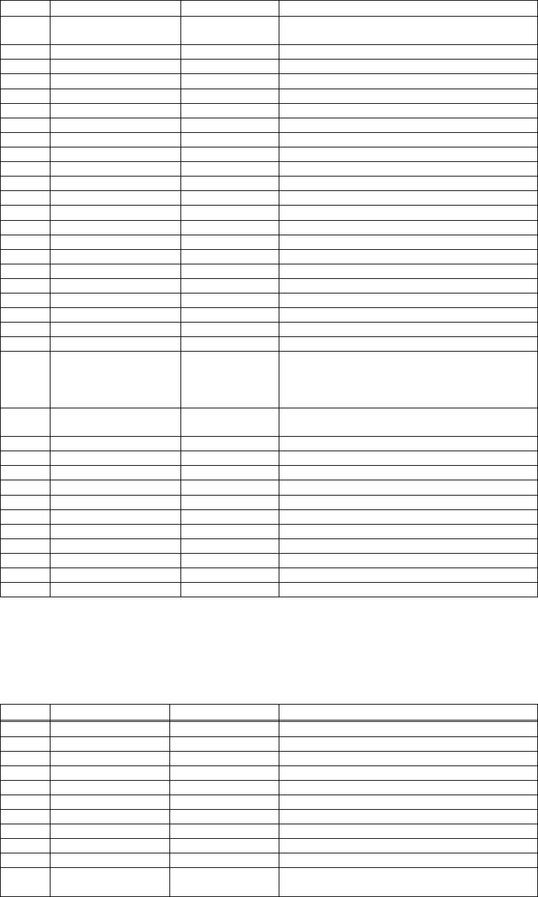
Pin # Signal Type Function/Notes
126 HPB_PRESENCE_
DETECT
Input Pulled down by HPB when HPB is present
127 HPB_SPI_CLK Output Dedicated SPI_CLK for HPB
128 GND
129 NC
130 GND
131 SPI_A0 Output SPI, to PS&PA
132 GND
133 NC
134 SPI_A1 Output SPI, to PS&PA
135 SPI_A2 Output SPI, to PS&PA
136 GND
137 SPI_A3 Output SPI, to PS&PA
138 GND
139 NC
140 SPI_MOSI Output SPI
141 SPI_MISO Input SPI
142 GND
143 NC
144 GND
145 PS1_SPI_EN Output
146 GND
147 NC
148 PS1_FAULT Input Indicates to XCVR Control board that the
Power supply detected a fault condition and
to write the condition to its EEPROM before
it goes off-line.
149 PS_PRESENCE_D
ETECT
Input Pulled down by PS when PS is present
150 GND
151 PS_SPI_CLK Output Dedicated SPI_CLK for PS
152 GND
153 NC
154 BP_ID1 Input/Output BP_ID1
155 NC
156 GND
157 EXT_REF Input
158 GND
159 NC
160 EXT_1PPS Input
RF Board Receiver Interconnect
The XCVR Control board interfaces to the RF board via a ribbon cable. The signals going to the RF board
Receiver’s interface are shown in the following Table.
RF Board Receiver Interconnect
Pin # Signal Type Function/Notes
1 Attn_Cntl_1_5 Output To RCVR from FPGA GPIO1_5
2 GND
3 Attn_Cntl_1_4 Output To RCVR from FPGA GPIO1_4
4 GND
5 Attn_Cntl_1_3 Output To RCVR from FPGA GPIO1_3
6 GND
7 Attn_Cntl_1_2 Output To RCVR from FPGA GPIO1_2
8 GND
9 Attn_Cntl_1_1 Output To RCVR from FPGA GPIO1_1
10 GND
11 Rcvr3_CU_Cntl Output switch control for RX power
From Host