
User's Manual


Table Of Contents
APPLICANT: MOTOROLA EQUIPMENT TYPE: ABZ89FC5812
User / Operational Manual
Functional Description / Operation of Modules and Interconnect (Draft)
EXHIBIT D1-6
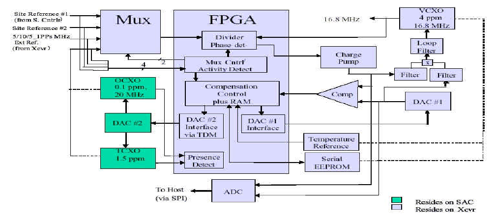
for one period to indicate this is the 1 PPS mark. The external reference sources are the Ext_Ref input, the two
CP2 links, and the OCXO which resides on the Supplemental Analog Card (SAC) (future development). The STIC
FPGA will automatically or manually (based on the STIC’s memory mapped register configuration) determine what
clock will be used as the reference. The same applies to the 1 PPS signals which come from a variety of sources.
The 1 PPS sources are the CP2_A, CP2_B, Ext_Ref, and Ext_1PPS. A block diagram of the Station Reference
Circuit can be seen in the Figure below.
The 16.8 MHz and external reference clocks will be divided down to 200 kHz internally in the STIC. These
resulting signals will be fed into an internal phase detector function block which will measure the phase difference
between the two signals. If the rising edge of the 200 kHz clock sourced from 16.8 MHz occurs later than the
rising edge of the 200 kHz clock sourced from the external reference, then the Phase_Det_U output of the FPGA
will pulse high for the duration of the phase difference. The high pulse on the Phase_Det_U will result in the
Charge Pump increasing its output voltage and increasing the VCXO frequency. The same scenario occurs if the
200 kHz clock sourced from 16.8 MHz occurs before the rising edge of the 200 kHz clock sourced from the
external reference. In this case the output of the Phase_Det_D pulses high for the duration of the difference. This
pulse will result in the Charge Pump decreasing the phase locked loop steering voltage and decreasing the VCXO
frequency.
The OCXO can be calibrated by applying a 5 or 10 MHz input signal (preferably a rubidium or equivalent) to the
reference BNC on the front panel of the XCVR. The STIC will automatically generate an interrupt (if not masked in
SW) to the DSP to indicate the presence of a valid 5 or 10 MHz input signal. The station reference will use this
signal to lock the 16.8 MHz VCXO. When locked it will record the steering voltage required to create this lock
condition by reading an ADC. Then the OCXO frequency reference will be used to lock the 16.8 MHz VCXO. The
VCXO steering voltage required for lock will also be recorded using the same ADC. The two VCXO steering
voltages will be compared. If the voltages are different, the OCXO steering voltage will be changed via the DAC.
The OCXO steering voltage will be changed until its output frequency creates the same VCXO steering voltage as
the VCXO steering voltage recorded when using the 5/10 MHz input reference. The OCXO DAC will reside on the
SAC. Data for the OCXO DAC will be placed on the DSP TDM bus TX Slot #8 (Outbound from DSP, Inbound to
SAC FGPA). The CST interface can be used to initiate the calibration process and indicate when the calibration is
complete. It can also record and timestamp the calibration date(s) and indicate when another calibration is
required.
Station Reference Block Diagram
The external references supported are the two 20 MHz clocks from the Site Controller, the external reference, and
the OCXO from the SAC board (future development). The STIC will monitor all of these signals and determine
which ones are not present or grossly out of tolerance. Each one of these fault conditions can be enabled to
create an interrupt to the DSP. The reference clock status can be determined by reading the STIC’s IRQ register
and/or the Clock Frequency Status registers. The FPGA can automatically determine which reference should use