
User's Manual


Table Of Contents
APPLICANT: MOTOROLA EQUIPMENT TYPE: ABZ89FC5812
User / Operational Manual
Functional Description / Operation of Modules and Interconnect (Draft)
EXHIBIT D1-6
Serial Interfaces and I/O
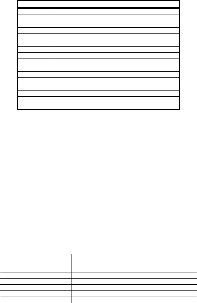
The following table shows the MPC8250’s communication port configuration for the control board. SCC1 will
support a synchronous RS232 port. It will also support the same V.24 functionality.
MPC8250 Communication Port Configuration
Port Interface supported
FCC1 10/100BaseT Ethernet
FCC2 10/100BaseT Ethernet
FCC3 10/100BaseT Ethernet
SCC1 Sync. RS232 / V.24
SCC2 Asynch RS232
SCC3 Transparent RX-only for PSM
SCC4 Unused
SMC1 Unused
SMC2 Front panel RS232
MCC1 Unused
MCC2 Unused
I2C I2C to 1-wire Bridge (to Dallas DS2433 EEPROM)
IDMA2 IDMA2 (DSP)
IDMA3 IDMA3 (DSP)
IDMA4 IDMA4 (Compact Flash)
SPI SPI
The control board has 64 MB of total SDRAM in the form of two 32 MB(16Mx16) devices. It supports a total of two
separate Flash memory banks, one bank for boot and one for application code. It also supports a CompactFlash
memory card. CompactFlash I/O cards are not supported. The Control board supports both Type I and Type II
form factor cards.
Reset Configuration
The front panel has one switch. The switch provides two functions, Access Disable and Reset. The Front Panel
switch is debounced for 16-32 ms. An Access Disable function will occur if the switch is pressed for less than 1
second but greater than the debounce time. A Reset sequence will occur if the switch is pressed for greater than
3 seconds. The reset sequence will consist of a Pre-Reset signal after 3 seconds followed by the actual reset 1
second later. The Pre-reset signal is used to notify the MPC8250 that an HRESET* is coming and to gracefully
shutdown the processor before reset occurs.
The DSP is an industrial temperature StarCore (SC140) based MSC8101. Production parts will operate at the
highest core and CPM rates supported at the date of shipment. Initial devices have a maximum core frequency of
275 MHz but will run at 268.8 MHz with CPMs running about half that speed. Core voltages are 1.6 VDC and IO
voltages are 3.3 VDC. On chip memory size is 512 KB. The package is a 332 pin FC-PBGA. See the following
table for clock mode and frequency information.
DSP Clock Information
Clock Mode 06
DSP Clock Input 67.2 MHz
Core Clock 268.8 MHz
CPM Clock 134.4 MHz
System Bus Clock 67.2 MHz
SCC Clock 67.2 MHz
Clock Out 67.2 MHz
BRG Clock 16.8 MHz default, configurable in SCCR
Station Reference
The station reference clock is 16.8 MHz. This clock is derived from a VCXO and in normal operation is locked to
an external reference of 5 MHz, 10 MHz, 20 MHz, or 5 MHz / 1 PPS. The 5MHz_1PPs signal is a 5 MHz signal
with an embedded 1 PPS clock. Typically the duty cycle of the clock is 25%. The duty cycle will change to 75%