
Specifications


Intel
®
810E2 Chipset Platform
R
108 Design Guide
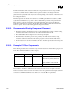
The following figure shows the recommended reference resistor placement and connections.
Figure 67. Recommended RAMDAC Reference Resistor Placement and Connections
R
set
Graphics Chip
Large Via or multiple Vias
straight down to ground plane
IREF
ball/pin
No toggling signals
should no toggling
signals should the R
set
resistor
Place the
resistor in close
proximity to the
IREF pin
Short, wide route connecting
the resistor to IREF pin
RAMDAC Reference Current
Setting Resistor 174
Ω
, 1±%,
1/16W, SMT, Metal Film
Ramdac1.vsd
3.26. DPLL Filter Design Guidelines
The 810E2 chipset contains sensitive phase-locked loop circuitry, the DPLL, that can cause excessive dot
clock jitter. Excessive jitter on the dot clock may result in a “jittery” image. An LC filter network
connected to the DPLL analog power supply is recommended to reduce dot clock jitter.
The DPLL bandwidth varies with the resolution of the display and can be as low as 100 kHz. In addition,
the DPLL jitter transfer function can exhibit jitter peaking effects in the range from 100 kHz to a few
megahertz. A low-pass LC filter is recommended for the display PLL analog power supply designed to
attenuate power supply noise with frequency content from 100 kHz and above so that jitter amplification
is minimized.
The following figure is a block diagram showing the recommended topology of the filter connection
(parasitics not shown). The display PLL analog power rail (VCCDA) is connected to the board power
plane through an LC filter. The RAMDAC analog power rails (VCCDACA1 and VCCDACA2) are
connected directly to the 1.8V board power plane.