TABLE OF CONTENTS SECURE MICROCONTROLLER USER’S GUIDE . . . . . . . . . . . . . . . . . . . . . . . . . . . . . . . . . . . . . . . . . 1 Section 1 Introduction . . . . . . . . . . . . . . . . . . . . . . . . . . . . . . . . . . . . . . . . . . . . . . . . . . . . . . . . . . . . . . . . . . . . . . . . . . 2 Section 2 Selection Guide . . . . . . . . . . . . . . . . . . . . . . . . . . . . . . . . . . . . . . . . . . . . . . . . . . . . . . . . . . . . . . . . . . . . . . .
USER’S GUIDE • Dedicated memory bus, preserving four 8–bit ports SECTION 1: INTRODUCTION The Secure Microcontroller family is a line of 8051–compatible devices that utilize nonvolatile RAM (NV RAM) rather than ROM for program storage. The use of NV RAM allows the design of a “soft” microcontroller which provides a number of unique features to embedded system designers.
USER’S GUIDE LARGE NONVOLATILE MEMORY other parallel loading protocols as well. In–system loading allows a system to be configured during final system test. A user can load custom software, diagnostic routines, or calibration constants. If something changes or new features arise, the system can then be reprogrammed while in the field. Soft Microprocessor chips provide nonvolatile memory control for standard CMOS SRAM. Modules combine the microprocessor chip with memory and lithium backup.
USER’S GUIDE PRODUCT DESCRIPTION • Built–in NV RAM of 8K x 8 or 32K x 8 All devices listed below have the standard 8051 family feature set listed once here for convenience, but not repeated for each device.
USER’S GUIDE DS2251T 128K Soft Microcontroller Module • Security is active at all times The DS2251T is a SIMM based on the DS5001. It provides up to 128K bytes of on–board NV RAM and has the Byte–wide bus available at the connector. This is used with the decoded peripheral enables for memory mapped peripherals such as a UART or A/D converter. The real–time clock is a parallel access type with interrupt capability.
USER’S GUIDE SECTION 2: SELECTION GUIDE controller family are fully static and can be run as slow as desired. The following configurations are available.
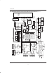
USER’S GUIDE SECTION 3: SECURE MICROCONTROLLER ARCHITECTURE Introduction B Register The major function of the B register is as a source and destination register during multiply and divide instructions. It may also be used as a scratchpad register. The Secure Microcontroller family is based on an 8051 compatible core with a memory interface and I/O logic build around it. Many functions are identical to standard 8051s and are documented here for completeness.
050396 7/173 8 RST EA ALE PSEN PORT 2 LATCH TIMING AND CONTROL INSTRUCTION REGISTER 8 8 XTAL1 128 SCRATCH– PAD REGISTERS IDR ADDR.
USER’S GUIDE Parallel I/O Scratchpad RAM and certain Special Function registers during a power down condition. Four SFR’s provide access for the four parallel I/O port latches. These I/O ports are denoted as P0, P1, P2, and P3. A total of 32 bits of parallel I/O is available through these I/O ports.
USER’S GUIDE Watchdog Timer RAM. The firmware provides Serial Bootstrap Load operation via the on–chip serial port. The internal ROM is not accessible by the user and performs the loading function only when the device is strapped for operation in the Program mode. The ROM becomes transparent to the user once loading is complete and has no effect on the memory map.
USER’S GUIDE SECTION 4: PROGRAMMER’S GUIDE cess a second RAM, but this was restricted to data memory only. The DS5001 series can partition two 32K byte SRAMs, or even one 128K x 8 SRAM. Common elements of the programming model are given below, with individual differences highlighted. The Secure Microcontroller uses nonvolatile RAM technology for both Program and Data memory. It uses NV SRAM in place of ROM by write protecting and decoding memory segments that a user designates as Program memory.
USER’S GUIDE The Scratchpad Registers are general purpose data storage RAM. They are commonly used for temporary storage of a small number of variables when high– speed access is needed. Off–chip RAM (MOVX) is used when the quantity of data is larger than 128 bytes. The Scratchpad Registers are lithium backed and will be preserved in the absence of power. A second use of the Scratchpad area is for the programmer’s stack.
USER’S GUIDE The 8051 instruction set allows efficient (single cycle) access to variables when using the Working Registers. These are a group of four 8–byte banks of Scratchpad RAM. The active Working Registers are referred to as R0–R7. They reside between location 00h and 1Fh, depending on which bank is currently selected. Two bits in the Special Function Register PSW called R1 (PSW.4) PSW.4–3 ; R1–R0 Register Bank Select and R0 (PSW.3) are used to determine which is the active bank.
USER’S GUIDE DS5000 Series Memory Organization Bus. Nonvolatile RAM access will occur when the logical address lies in one of the shaded regions. These are program addresses below the Partition address, data addresses above the Partition and below the Range address, or data addresses between 0 and the Range when ECE2 is set to a logic 1. Note that when using ECE2 to force data access, the CE2 RAM will be selected instead of the CE1 RAM.
USER’S GUIDE DS5000 SERIES MEMORY MAP Figure 4–3 ECE2=0 7FFFh 1FFFh BYTE–WIDE BUS ACCESS PARTITION ADDR. ÑÑÑÑÑÑ ÑÑÑÑÑÑ ÑÑÑÑÑÑ ÑÑÑÑÑÑ ÑÑÑÑÑÑ ÑÑÑÑÑÑ ECE2=1 FFFFh 64K 32K RANGE ADDR.
USER’S GUIDE case is to select a Range of 8K, and to choose a Partition of greater than 8K. This will result in the Range as the limiting factor. Addresses above the Range will automatically be deflected to the Expanded bus. No data memory will be allocated in NV RAM for this configuration. tion, the Partition can be selected or modified by the application software and CE2 is normally software controlled. However, in either case, the MCON SFR is used to choose these settings.
USER’S GUIDE MCON.3: RA32/8 “Range Address”: Sets the maximum usable address on the Byte–wide bus. RA32/8 = 0 sets Range Address = 1FFFH (8K); RA32/8 = 1 sets Range Address = 7FFFH (32K) Initialization: Set to a 1 on a No VLI Power On Reset and when the Security Lock bit (SL) is cleared to a 0 from a previous 1 state. Remains unchanged on all other types of resets. Read Access: May be read normally anytime.
USER’S GUIDE which configuration is used. The Range function determines how much total memory is connected to the Byte–wide bus. The user must identify the total RAM size using the Range bits RG1 and RG0. RG1 is located at MCON.3 and RG0 is located at RPCTL.0. These Range bits are selected during the Bootstrap Loading process and can not be modified by the application software. The Table below shows the Range values that can be selected when PM=0 (Partitionable).
USER’S GUIDE PARTITIONABLE MEMORY MAP FOR DS5001/DS5002 SERIES Figure 4–5 PES=0 FFFFh 64K RANGE ADDRESS BYTE–WIDE BUS ACCESS PARTITION ADDR. BYTE–WIDE BUS ACCESS 0000 PROGRAM MEMORY DATA MEMORY LEGEND: BYTE–WIDE ACCESS = (NONVOLATILE RAM) ÏÏ ÏÏ = EXPANDED BUS ACCESS ON PORTS 0 AND 2 The non–partitionable mode allows the maximum amount of memory to be used on the Byte–wide bus.
USER’S GUIDE Any address that does not fall into the Byte–wide bus area is routed to the Expanded bus of Ports 0 and 2. This could only occur for the first two settings. Note that a single 128K device is the least expensive in terms of component cost and size. In this case, all memory addressable by the DS5001 is stored in a nonvolatile 128K x 8 SRAM. When the MSEL pin is grounded, the device automatically converts CE1 to a chip enable, CE2 to A16, CE3 to A15, and CE4 is unused.
USER’S GUIDE On occasion, a memory mapped peripheral is needed that interfaces directly to an 8051 multiplexed bus. When this occurs, MOVX instructions can be forced to use the Expanded bus in any mode with the EXBS bit (RPCTL.5). Setting this bit to a logic one forces all MOVX instructions to the Expanded bus. While EXBS=1, the entire 64K data memory map is accessed in this way. Clearing EXBS will cause the microcontroller to revert to its selected configuration.
USER’S GUIDE DS5001/DS5002 SERIES MCON REGISTER Figure 4–8 PA3 PA2 PA1 PA0 RG1 PES PM Bit Description: MCON.7–4: PA3–0 Partition Address. When PM=0, this address specifies the boundary between program and data memory in a continuous space. Initialization: Unaffected by watchdog, external, or power–up resets. Set to 1111B on a No VLI reset. Read Access: Can be read normally at any time. Write Access: Timed Access Protected.
USER’S GUIDE DS5001/DS5002 SERIES RPCTL REGISTER BITS AFFECTING MEMORY Figure 4–9 RNR ––– EXBS AE IBI DMA RPCON RG0 Bit Description: RPCTL.5: EXBS The Expanded Bus Select routes data memory access (MOVX) to the Expanded bus formed by ports 0 and 2 when set. Initialization: Cleared after all resets. Read Access: Can be read at any time. Write Access: Can be written at any time. RPCTL.4: AE Access Enable is used when a software reload is desired without using Program Load mode.
USER’S GUIDE Application software always has unrestricted read/write access to the nonvolatile RAM designated as data memory. This is the memory that lies above the Partition address and below the Range address (the non–partitionable configuration of the DS5001 will be addressed separately). Data memory is read or written using the MOVX instruction. Only the area designated as program memory can not be altered.
USER’S GUIDE MOV TA, #0AAh ; TIMED ACCESS MOV TA, #55h ; TIMED ACCESS 2 MOV MCON, #10001010b ; SET PAA BIT . ; USER’S CODE TO LOAD . ; RAM USING MOVX . .
USER’S GUIDE AE bit. Note that AE requires software to use a Timed Access procedure to alter it. This method allows a user to alter program memory in a non–partitionable mode. Data memory can be initialized by application software at any time. Since full read/write access is available, no special provisions are needed. SOFT RELOAD OF A DS5001/DS5002 When application software decides that it should reprogram a portion of memory, the software must convert the target area into data memory.
USER’S GUIDE MOV TA, #0AAh MOV TA, #55h MOV MCON, ; TIMED ACCESS ; TIMED ACCESS 2 #00011000b ; SET PARTITION TO 1000h | ; USER’S CODE TO LOAD | ; RAM USING MOVX | | MOV TA, #0AAh ; TIMED ACCESS MOV TA, #55h MOV MCON, #10101000b ; LOAD NEW PARTITION OF A000h ; TIMED ACCESS 2 RELOADING A DS5001/DS5002 SERIES DEVICE Figure 4–11 FFFFh RANGE (64K) DATA MEMORY SPACE DATA MEMORY SPACE DATA MEMORY SPACE A000h NEW PARTITION (40K) PROGRAM MEMORY SPACE 4000h PROGRAM MEMORY SPACE 1000h OLD
USER’S GUIDE Special Function Registers spectively. In addition, the Secure Microcontroller requires a Timed Access procedure before allowing software to modify the STOP mode bit (PCON.1). This is to prevent errant software from creating a situation that the Watchdog Timer can not recover from. The remaining SFRs are either identical to the 8051 or new to the architecture. The Secure Microcontroller uses Special Function Registers (SFRs) to control most functions.
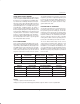
USER’S GUIDE DS5000 SERIES SPECIAL FUNCTION REGISTER MAP Figure 4–12 DIRECT BYTE ADDRESS SPECIAL FUNCTION REGISTER SYMBOL (MSB) (LSB) BIT ADDRESS 0F0H F7 F6 F5 F4 F3 F2 F1 F0 B 0E0H E7 E6 E5 E4 E3 E2 E1 E0 ACC C AC F0 RS1 RS0 OV 0D0H D7 D6 D5 D4 D3 D2 D1 D0 0C7H P TA NOT BIT ADDRESSABLE PA3 PA2 PA1 0C6H PA0 RA32/8 ECE2 PAA SL MCON NOT BIT ADDRESSABLE RWT PSW PS PT1 PX1 PT0 PX0 0B8H BF – – BC BB BA B9 B8 IP 0B0H B7 B6 B5 B4 B3 B2 B1
USER’S GUIDE DS5001/DS5002 SERIES SPECIAL FUNCTION REGISTER MAP Figure 4–13 DIRECT BYTE ADDRESS 0F0H 0E0H (MSB) F7 BIT ADDRESS F6 F5 0D0H F3 F2 F1 B ACC E7 E6 E5 E4 E3 E2 E1 E0 ST6 ST5 ST4 IA0 F0 IBF 0BF RNR ––– EXBS DMA RPC RG0 DF DE DD DC DB DA D9 D8 C AC F0 RS1 RS0 OV D7 D6 D5 D4 D3 D2 NOT BIT ADDRESSABLE AE IBI 0CFH NOT BIT ADDRESSABLE 0C7H NOT BIT ADDRESSABLE PA3 PA2 PA1 PA0 RG1 SPECIAL FUNCTION REGISTER SYMBOL F0 ST7 0DAH 0D8H F4 (LS
USER’S GUIDE POWER CONTROL REGISTER Label: PCON Register Address: 087H D7 D6 D5 D4 D3 D2 D1 D0 SMOD POR PFW WTR EPFW EWT STOP IDL Bit Description: PCON.7 SMOD “Double Baud Rate”: When set to a 1, the baud rate is doubled when the serial port is being used in modes 1, 2, or 3. Initialization: Cleared to a 0 on any reset. Read Access: Can be read normally at any time. Write Access: Can be written normally at any time. PCON.
USER’S GUIDE PCON.3: EPFW “Enable Power Fail Interrupt”: Used to enable or disable the Power Fail Interrupt. When EPFW is set to a 1, it will be enabled; it will be disabled when EPFW is cleared to a 0. Initialization: Cleared to a 0 on any type of reset. Read Access: Can be read normally anytime. Write Access: Can be written normally anytime. PCON.2: EWT “Enable Watchdog Timer”: Used to enabled or disable the Watchdog Timeout Reset.
USER’S GUIDE TIMER CONTROL REGISTER Label: TCON Register Address 088H D7 D6 D5 D4 D3 D2 D1 D0 TF1 TR1 TF0 TR0 IE1 IT1 IE0 IT0 Bit Description: TCON.7: TF1 “Timer 1 Overflow Flag”: Status bit set to 1 when Timer 1 overflows from a previous count value of all 1’s. Cleared to 0 when CPU vectors to Timer 1 interrupt service routine. Initialization: Cleared to 0 on any type of reset. TCON.6: TR1 “Timer 1 Run Control”: When set to a 1 by software, Timer 1 operation will be enabled.
USER’S GUIDE TCON.0: IT0 “Interrupt 0 Type Select”: When set to 1, 1–to–0 transitions on INT0 will be used to generate interrupt requests from this pin. When cleared to 0, INT0 is level–activated. Initialization: Cleared to a 0 on any type of reset. TIMER MODE REGISTER Label: TMOD Register Address: 089H D7 D6 D5 D4 D3 D2 D1 D0 GATE C/T M1 M0 GATE C/T M1 M0 Bit Description: TMOD.7 (Timer 1); TMOD.
USER’S GUIDE SERIAL CONTROL REGISTER Label:SCON Register Address: 098H D7 D6 D5 D4 D3 D2 D1 D0 SM0 SM1 SM2 REN TB8 RB8 TI RI Bit Description: SCON.7, SCON.
USER’S GUIDE Initialization: Cleared to a 0 on any type of reset. SCON.0: RI “Receive Interrupt”: Status bit used to signal that a serial data word has been received and loaded into the receive buffer register. In mode 0, it is set at the end of the 8th bit time. It is set at the mid–bit time of the incoming stop bit in all other modes of a valid received word according to the state of SM2.
USER’S GUIDE INTERRUPT PRIORITY REGISTER Label:IP Register Address: 0B8H D7 D6 D5 D4 D3 D2 D1 D0 RWT – – PS PT1 PX1 PT0 PX0 Bit Description: IP.7: RWT “Reset Watchdog Timer”: When set to a 1, the Watchdog Timer count will be reset and counting will begin again. The RWT bit will then automatically be cleared again to 0. Writing a 0 into this bit has no effect. Initialization: Cleared to a 0 on any reset. Read Access: Cannot be read.
USER’S GUIDE DS5001 CRC REGISTER Label: CRC RNGE3 Register Address: 0C1H RNGE2 RNGE1 RNGE0 ––– ––– MDM CRC Bit Description: CRC.7–4 RNGE3–0 Determines the range over which a power–up CRC will be performed. Addresses are specified on 4K boundaries. Initialization: Reset to 0 on a No VLI reset. Read Access: Can be read at any time. Write Access: Cannot be written by the application software. Can only be written via the Bootstrap Loader. CRC.
USER’S GUIDE DS5000 MEMORY CONTROL REGISTER Label:MCON Register Address: 0C6H D7 D6 D5 D4 D3 D2 D1 D0 PA3 PA2 PA1 PA0 RA32/8 ECE2 PAA SL Bit Description: MCON.7–4: PA3–0 “Partition Address”: Used to select the starting address of Data Memory on the Byte–wide bus. Program space lies below the partition address.
USER’S GUIDE Read Access: May be read normally anytime. Write Access: Cannot be modified by the application software; can only be written via the Bootstrap Loader. MCON.2: ECE2 “Enable Chip Enable 2”: Used to enable or disable the CE2 signal for the Byte–wide bus data memory. This bit should always be cleared to 0 in the DS5000, DS5000-32, DS2250–8 and DS2250–32 versions. Initialization: Cleared to 0 only during a No VLI Power On Reset. Read Access: Read normally anytime.
USER’S GUIDE Write Access: Timed Access Protected. Cannot be written by the application software if set to 0000B by the serial loader. If a 0000B is written via the serial loader and the security lock is set, the Partition will become 1111B. The same will occur if write access is available and application software writes a 0000B. In addition, these bits will be set to 1111B if security lock is cleared. MCON.3: RG1 One of two bits that determine the range of program space.
USER’S GUIDE PROGRAM STATUS WORD REGISTER Label:PSW Register Address: 0D0H D7 D6 D5 D4 D3 D2 C AC F0 RS1 RS0 OV D1 D0 P All of the bits in PSW except parity are read/write and are cleared to 0 on any type of reset. The Parity bit is read only and is cleared to 0 on any type of reset. Bit Description: PSW.7: C “Carry”: Set when the previous operation resulted in a carry (during addition) or a borrow (during subtraction). Otherwise cleared. PSW.
USER’S GUIDE DS5001/DS5002 RPC CONTROL REGISTER Label: RPCTL RNR Register Address: 0D8H ––– EXBS AE IBI DMA RPCON RG0 Bit Description: RPCTL.7 RNR When internal hardware sets this read–only bit to a 1, a new value may be read from the random number generator register of the DS5001/DS5002 (RNR;0CFh). This bit is cleared when the random number is read, and approximately 160 µs are required to generated the next number. Initialization: Cleared after all resets.
USER’S GUIDE Read Access: Can be read anytime. Write Access: Can be written when the RPC mode is enabled (RPCON=1). RPCTL.1 RPCON Enable the RPC 8042 I/O protocol. When set, port 0 becomes the data bus, and port 2 becomes the control signals. Initialization: Cleared on all resets. Read Access: Can be read at any time. Write Access: Can be written at any time. RPCTL.0 RG0 This is a Range bit which is used to determine the size of the program memory space. Its usage is shown above.
USER’S GUIDE Read Access: Can be read by DS5001/DS5002 and host CPU when in RPC mode. Write Access: Can be written by the DS5001/DS5002 when in RPC mode. RPS.1: IBF Input Buffer Full Flag is set following a write by the external host, and is cleared following a read of the DBBIN by the DS5001/DS5002. Initialization: Cleared when RPC=0. Read Access: Can be read by DS5001/DS5002 and host CPU when in RPC mode. Write Access: Written automatically as part of the RPC communication.
USER’S GUIDE INSTRUCTION SET Introduction Direct Addressing Direct Addressing is the only mode available for use on operands within the Special Function registers. Addressing of bytes may also be used to access the 128 Internal Data registers. The Secure Microcontroller executes an instruction set which is object code compatible with the industry standard 8051 microcontroller.
USER’S GUIDE to +128) which is added to the PC to determine the destination address which will be branched to when the tested condition is found to be true. The PC points to the Program Memory location immediately after the Branch instruction when the offset is added. If the condition is found to be not true, then program execution continues from the address of the following instruction. The 16–bit DPTR register may be used to access any Data Memory location within the 64K byte space.
USER’S GUIDE Program Status Flags All of the Program Status flags are contained in the PSW register. Instructions which affect the states of the flags are summarized below.
USER’S GUIDE SECTION 5: MEMORY INTERCONNECT the user must connect this Byte–wide bus to the RAM as shown in this section. In module form, the bus is connected inside the package. Table 5–1 shows some of the preferred RAM choices. Note that any standard SRAM will work, but data retention lifetime is dependent on RAM data retention current and battery capacity. Lower currents naturally allow the use of smaller batteries. This is covered in detail in Section 6.
USER’S GUIDE MEMORY INTERCONNECT OF THE DS5000FP Figure 5–1 32K x 8 SRAM DS5000FP 13 +5v 54 VCC VCCO 12 VLI R/W 10 27 CE1 74 20 +3v ÇÇÇ ÇÇ Ç ÇÇ ÇÇ ÇÇÇ ÇÇ Ç ÇÇ ÇÇ ÇÇÇ ÇÇ Ç ÇÇ ÇÇÇ ÇÇ Ç ÇÇ PORT0 PORT1 BA14–BA0 BD7–BD0 28 WE CS ÓÓÓÓÓÓÓÓÓÓ Ó ÓÓÓÓÓÓÓÓÓÓ Ó ÔÔ ÔÔÔÔÔÔÔÔÔ Ô ÔÔ ÔÔÔÔÔÔÔÔÔ Ô A14–A0 D7–D0 14 PORT2 VCC EA 73 CE2 78 GND +5v PORT3 52 GND DS5000 SERIES MODULE BLOCK DIAGRAM Figure 5–2 DS5000(T), DS2250(T) DS5000FP 40–PINS ÇÇ ÇÇ ÇÇÇÇ ÇÇ ÇÇ ÇÇ ÇÇÇÇ ÇÇ ÇÇ ÇÇ ÇÇÇÇ ÇÇÇÇ ÇÇ ÇÇ
USER’S GUIDE In the non–partitionable case, the DS5001FP can be connected to three or four 32K x 8 SRAMs. The four RAM case is shown in Figure 5–4. Each RAM has its own chip enable. To use three RAMs, simply omit the unused chip enable (CE2 or 4) as described in Section 4. In other ways, this hardware configuration is similar to the Partitionable mode discussed above. While this provides the full 128K bytes of memory, it requires more space and cost than the version shown in Figure 5–5.
USER’S GUIDE MEMORY INTERCONNECT OF THE NON–PARTITIONABLE DS5001FP, DS5002FP Figure 5–4 32K X 8 SRAM DS5001FP/DS5002FP 13 +5V 54 VCC VCCO VLI ÇÇ ÇÇ ÇÇ ÇÇ ÇÇÇÇ ÇÇ ÇÇ ÇÇ ÇÇ ÇÇ ÇÇ ÇÇ ÇÇ ÇÇ ÇÇ ÇÇÇÇ ÇÇ ÇÇ ÇÇ ÇÇ R/W +3V CE1 BA14–BA0 PORT0 PORT1 BD7–BD0 28 10 27 CE2 CE3 PORT3 CE4 GND 20 14 OE 22 D7–D0 GND 2 63 62 27 +5V CS A14–A0 28 MSEL VCC WE ÓÓÓÓÓÓÓÓÓ ÔÔÔÔÔÔÔÔÔ ÓÓÓÓÓÓÓÓÓ ÔÔÔÔÔÔÔÔÔ ÓÓÓÓÓÓÓÓÓ ÔÔÔÔÔÔÔÔÔ ÓÓÓÓÓÓÓÓÓ ÔÔÔÔÔÔÔÔÔ ÓÓÓÓÓÓÓÓÓ ÔÔÔÔÔÔÔÔÔ ÓÓÓÓÓÓÓÓÓ ÔÔÔÔÔÔÔÔÔ ÓÓÓÓÓÓÓÓÓ ÔÔÔÔÔÔÔÔÔ Ó
USER’S GUIDE MEMORY INTERCONNECT USING THE 128K SRAM Figure 5–5 128K x 8 SRAM DS5001FP/DS5002FP 13 +5v 54 VCC VCCO VLI R/W +3v Ç Ç ÇÇÇ ÇÇÇ Ç Ç Ç Ç ÇÇÇ Ç Ç ÇÇÇ Ç Ç Ç Ç ÇÇÇ Ç Ç Ç Ç 52 CE1 CE2 PORT0 PORT2 PORT3 28 10 27 74 20 2 2 VCC WE 30 CS1 CS2 A16 OE 22 ÓÓ ÓÓÓÓÓÓÓÓÓ ÓÓ Ô ÔÔ ÔÔÔÔÔÔÔÔÔ Ô ÔÔ CE3 PORT1 12 63 31 A15 BA14–BA0 A14–A0 BD7–BD0 D7–D0 16 GND MSEL GND 14 a DS5001FP. The DS2252T Secure Micro Stik is based on the DS5002FP.
USER’S GUIDE DS2251T–128 BLOCK DIAGRAM Figure 5–6 DS2251T DS5001FP 128K X 8 SRAM 72 PINS ÇÓÓÓÓÓÓÓÓÓÓÓÓÓÓÓÓÓ Ç ÇÇÇÇÇÇ ÓÓÓÓÓÓÓÓÓÓÓÓÓÓÓÓÓ Ç ÇÇÇÇÇÇ ÔÔÔÔÔÔÔÔÔÔÔÔÔÔÔÔÔ Ç ÓÓÓÓÓÓÓÓÓÓÓÓÓÓÓÓÓ ÇÇÇÇÇÇ Ç ÔÔÔÔÔÔÔÔÔÔÔÔÔÔÔÔÔ ÓÓÓÓÓÓÓÓÓÓÓÓÓÓÓÓÓ ÇÇÇÇÇÇ Ç ÔÔÔÔÔÔÔÔÔÔÔÔÔÔÔÔÔ ÓÓÓÓÓÓÓÓÓÓÓÓÓÓÓÓÓ ÇÇÇÇÇÇ Ç ÔÔÔÔÔÔÔÔÔÔÔÔÔÔÔÔÔ ÓÓÓÓÓÓÓÓÓÓÓÓÓÓÓÓÓ ÇÇÇÇÇÇ Ç ÔÔÔÔÔÔÔÔÔÔÔÔÔÔÔÔÔ ÓÓÓÓÓÓÓÓÓÓÓÓÓÓÓÓÓ ÔÔÔÔÔÔÔÔÔÔÔÔÔÔÔÔÔ ÓÓÓÓÓÓÓÓÓÓÓÓÓÓÓÓÓ ÔÔÔÔÔÔÔÔÔÔÔÔÔÔÔÔÔ ÓÓÓÓÓÓÓÓÓÓÓÓÓÓÓÓÓ ÔÔÔÔÔÔÔÔÔÔÔÔÔÔÔÔÔ ÓÓÓÓÓÓÓÓÓÓÓÓÓÓÓÓÓ ÔÔÔÔÔÔÔÔÔÔÔÔÔÔÔÔÔ ÓÓÓÓÓÓÓÓÓÓÓÓÓÓÓÓÓ ÔÔ
USER’S GUIDE DS2252T–32 BLOCK DIAGRAM Figure 5–7 DS2252T DS5002FP 32K X 8 SRAM 40 PINS ÇÇÇÇÇ ÇÇ ÇÇÇÇÇÇ ÇÇ ÇÇ ÇÇÇÇÇ ÇÇ ÇÇÇÇÇ ÇÇ ÇÇÇÇÇ ÇÇ ÇÇÇÇÇ ÇÇ VCCO VCC (8) ADDR PORT0 (8) DATA PORT1 CE1 (8) PORT2 (8) ÓÓÓÓÓÓÓ ÔÔÔÔÔÔÔ ÓÓÓÓÓÓÓ ÔÔÔÔÔÔÔ ÓÓÓÓÓÓÓ ÔÔÔÔÔÔÔ ÓÓÓÓÓÓÓ ÔÔÔÔÔÔÔ ÓÓÓÓÓÓÓ ÔÔÔÔÔÔÔ ÓÓÓÓÓÓÓ ÔÔÔÔÔÔÔ ÓÓÓÓÓÓÓ ÔÔÔÔÔÔÔ ÓÓÓÓÓÓÓ ÔÔÔÔÔÔÔ ÔÔÔÔÔÔÔ REAL TIME CLOCK PORT3 ALE RST XTAL1 XTAL2 PE1 PROG SDI GND VLI +3V 050396 54/173 55
USER’S GUIDE SECTION 6: LITHIUM/BATTERY BACKUP tained at a logic high state with lithium power, but non– backed chip enables follow VCC down. Individual product differences should be observed. Maintaining chip enables at an inactive level and lowering the power supply to approximately +3V causes the NV RAM to enter a data retention state. Thus the combination retains data for a long period as the circuits draw a very small current from the lithium cell.
USER’S GUIDE POWER SUPPLY SLEW RATE Figure 6–1 40 µs, 130 µs VCC VCCMIN VLI LITHIUM CURRENT Each time VCC is restored, the lithium backed functions will remain as they were left. A result is that many of these values are not altered on a reset condition except for the ‘no battery reset’. In the documentation, this is referred to as ‘No VLI reset’. This will occur after the first time VCC is applied to the microprocessor. The ‘no battery reset’ state is documented in the section on resets.
USER’S GUIDE 10 years depending on the user’s actual environment and design goals. backed circuits, if any. In a Dallas module, these are screened for combination with the appropriate battery. In using a chip, the user must balance the size/cost of a larger lithium cell with the data retention current/cost of SRAMs. The system lifetime can be determined from three parameters: 1) Data retention current, 2) Lithium cell capacity, 3) Lithium self–discharge.
USER’S GUIDE LITHIUM BATTERY USAGE incorporate the Freshness Seal. The Freshness Seal electrically isolates the lithium cell from any external loading. Thus even in the absence of power, the SRAM and Real–Time Clock leakage currents will not be drawn from the lithium cell for as long as the Freshness Seal is applied. In the vast majority of applications, lithium batteries provide a reliable means of backing up data and configuration.
USER’S GUIDE SECTION 7: POWER MANAGEMENT Introduction Figure 7–1. The instruction which sets this bit will be the last instruction executed before Idle mode operation begins. Once in the Idle mode, the microprocessor preserves the entire CPU status including the Stack Pointer, Program Counter, Program Status Word, Accumulator, and RAM. There are two ways to terminate the Idle mode. The first is from an interrupt which has been previously enabled prior to entering Idle mode.
USER’S GUIDE Write Access: Cannot be written. PCON.3: EPFW “Enable Power Fail Interrupt”: Used to enable or disable the Power Fail Interrupt. When EPFW is set to a 1, it will be enabled; it will be disabled when EPFW is cleared to a 0. Initialization: Cleared to a 0 on any type of reset. Read Access: Can be read normally anytime. Write Access: Can be written normally anytime. PCON.1: STOP “Stop”: Used to invoke the Stop mode.
USER’S GUIDE The original contents of those Special Function registers that are initialized by a reset are lost. power fail condition so that the operational state of the processor can be saved just prior to entering the Data Retention. Voltage Monitoring Circuitry The voltage monitoring circuitry recognizes three voltage thresholds below nominal operating voltage. These thresholds are identified as VPFW (Power Fail Warning voltage), VCCmin (minimum operating voltage), and VLI (lithium supply) voltage.
USER’S GUIDE Power Fail Interrupt When power is once again applied to the system, the VCC voltage will eventually cross the VLI threshold. When this action is detected, the microprocessor will automatically switch its internal supply line from the lithium source back to the VCC pin. When VCC voltage eventually goes above the VCCmin threshold, the clock oscillator is allowed to start up and an internal Power On Reset cycle is executed.
USER’S GUIDE then it will remain cleared until the next time VCC goes below VPFW. threshold, the Power On Reset cycle will be executed as before. As a result, no special processing is required in software to accommodate this case. As long as the PFW flag is set, an interrupt condition is defined if EPFW is set. If the software executes a service routine in response to a PFW interrupt and exits the service routine with the PFW flag still set, then the processor will be immediately interrupted again.
USER’S GUIDE SECTION 8: SOFTWARE CONTROL Introduction Access register at location 0C7h. The first write should be a value of 0AAh and the second should be a value of 55H. After this sequence is performed, the protected bits may be modified. Upon receiving a 0AAH in the Timed Access register, two timers are initiated. The first timer allows two instruction cycles to write a 55H. This means a one– or two–cycle instruction may be used. If 55H is not written within two cycles, Timed Access is reset.
USER’S GUIDE This code allows the reset of the Watchdog Timer: MOV MOV SETB 0C7H,#0AAH 0C7H,#055H IP.7 ; 1st TA Value ; 2nd TA Value ; Reset Watchdog Timer 2 Cycles 1 Cycle The Watchdog Timer bit may have been set using ORL IP, #80H which takes two cycles.
USER’S GUIDE Watchdog Timer Timed Access provides a statistical protection. It is unlikely that randomly generated states will correctly match the sequence and timing required to bypass the Timed Access logic. Presented below is a brief justification for each bit that is protected by Timed Access. The on–chip Watchdog Timer provides a method of restoring proper operation during transients that cause the loss of controlled execution of software.
USER’S GUIDE watchdog 122,880 cycle counter. During this time, the bit may be read but attempts to clear the bit will fail. This condition will not be noticed if the Enable Watchdog Timer bit (EWT) is set, because the 8192 cycle count will be reset during the device reset triggered by the watchdog time–out. The bit may then be cleared, if desired, during application’s power–on reset routine.
USER’S GUIDE WATCHDOG TIMER CONTROL BITS Bit Description: PCON.4: WTR “Watchdog Timer Reset” Set to a 1 when a Watchdog Timer timeout occurs. If Watchdog Timer Reset is enabled, this will indicate the cause of the reset. Cleared to 0 immediately following a read of the PCON register. Initialization: Set to a 1 after a Watchdog Timeout. Cleared to a 0 on a No–VLI Power On Reset. Remains unchanged during other types of resets. Read Access: May be read normally anytime.
USER’S GUIDE blocks over which the CRC calculation is performed. For example, if the nibble is set to 0001b, the CRC range is from 0000 to 0FFFh. Once the LSB of the CRC register is set, the loader “I” command will cause the CRC of the specified block to be computed. The result is automatically stored in the last two bytes of the specified block. These bytes should not be used by the application. This computation will be correct provided that the CRC range is less than or equal to the partition if PM=0.
USER’S GUIDE CRC CODE EXAMPLE Figure 8–3 This routine tests the CRC–16 circuit in the DS5001FP crcmsb crclsb equ equ 0C3h 0C2h org 00h ;after reset, CRC regs = 0000 mov mov mov p2,crcmsb p3,crclsb crclsb, #075h mov mov mov mov mov mov mov mov mov crclsb, #08Ah crclsb, #00Bh crclsb, #075h crclsb, #0C7h crclsb, #0AAh crclsb, #075h crclsb, #0C7h crclsb, #055h crclsb, #043h ;p2=00 read crcmsb register ;p3=00 read crclsb register ;check crc register operation ;data in = 75 result = E7C1 ;data in = 8A
USER’S GUIDE SECTION 9: FIRMWARE SECURITY Also included are guidelines to using microcontroller security within the framework of total system security. One of the most unique features of the Secure Microcontroller is its firmware security. The family far surpasses the standard offering of ROM based microcontrollers in keeping system attackers or competitors from viewing the contents of memory.
USER’S GUIDE SECURITY LOCK Thus the instantaneous erasure of the Encryption Key renders the contents of memory useless since it can no longer be properly deciphered. Ordinarily, the easiest way to dump (view) the memory contents of a Secure Microcontroller is using the Bootstrap Loader. On request, the Loader will transfer the contents of memory to a host PC. This is prevented by the Security Lock. The lock is the minimal security feature, available even in the DS5001.
USER’S GUIDE DS5000 SOFTWARE ENCRYPTION BLOCK DIAGRAM Figure 9–1 PROGRAM COUNTER DATA POINTER ENCRYPTED BYTEWIDE DATA BUS SECURE INTERNAL ADDRESS BUS ADDRESS ENCRYPTOR 15 EXTERNAL BYTEWIDE RAM BOOTSTRAP LOADER 40–BIT ENCRYPTION KEY SECURITY LOCK ENCRYPTED BYTEWIDE DATA BUS SECURE INTERNAL DATA BUS DATA ENCRYPTOR 8 DS5002 SOFTWARE ENCRYPTION BLOCK DIAGRAM Figure 9–2 PROGRAM COUNTER DATA POINTER ENCRYPTED BYTEWIDE DATA BUS SECURE INTERNAL ADDRESS BUS ADDRESS ENCRYPTOR 16 RANDOM NUMBER GENERATOR B
USER’S GUIDE The Data Encryptor operates in a similar manner to the address encryptor. As each byte including opcode, operand, or data is received during Bootstrap Loading, its value is scrambled prior to storing it in RAM. The value that is actually written in RAM is an encrypted representation. All values that are subsequently stored in RAM during execution also are encrypted. As each byte is read back to the CPU during execution, the internal Data Encryptor restores it to its original value.
USER’S GUIDE Encryption Algorithm Key during program loading. This Key must be selected prior to loading the microcontroller, as the memory will be encrypted as it is loaded. The Key selection process must be protected since an attacker that learns the Key can reproduce the user’s code. This would be done by loading the correct Key in an unlocked DS5000FP, attaching the encrypted memory chip, and dumping the code using the Bootstrap Loader.
USER’S GUIDE Dummy Bus Access switched according to a pseudo–random process. This is repeatable so that the execution always appears the same. During these pseudo–random cycles, the RAM is to all appearance read. Thus by repeatedly switching between real and dummy access, it is impossible to distinguish a dummy cycle from a real one. In analyzing bus activity, a large percentage of the memory fetches will be garbage that has no meaning.
USER’S GUIDE On–chip Vector RAM ing power applied to the VCCI pin. Activation of the SDI pin instantaneously clears the Security Lock initiating the sequence of events described above. In addition, power is momentarily removed from all Byte–wide bus interface signals including the VCCO pin, resulting in loss of data by the external RAM. Address and data lines are also pulled low to remove any excess charge that could help retain data in that RAM.
USER’S GUIDE Security Summary by Part This is used to prevent the Bootstrap Loader from dumping memory. Once locked, the Bootstrap Loader can not access the memory. Unlocking the DS5001 causes the Bootstrap Loader to write over the NV RAM. The RAM nature of the DS5001 product allows a user to vary security frequently and to manually destroy it if necessary. The preceding information outlined each of the security features.
USER’S GUIDE APPLICATION: ADVANCED SECURITY TECHNIQUES checksum. If one is needed, then check the minimum amount of memory and perform the check in non–sequential fashion. The Secure Microcontroller family has been used for numerous applications requiring security. Different levels of security are required depending on the sensitivity of the application and the value of the protected information.
USER’S GUIDE Change Code stored inside the Secure Microcontroller. This serializes the system. If the software ever finds a different serial number (or missing number) from the stored one, it can refuse to work. This would mean that the microprocessor had been moved. Perhaps most importantly, the user should reprogram portions of the Secure Microcontroller that deal with security. For example, if the microprocessor is performing DES, the user can change DES keys.
USER’S GUIDE SECTION 10: RESET CONDITIONS Reset Sources Certain actions are taken in all cases where a reset has been issued. Whenever any type of reset is executed, the ALE and PSEN quasi–bidirectional pins are configured as inputs. In addition, an internal reset line (IRST) is active continuously until the condition which is causing the reset has been removed. IRST will then go inactive and execution of the application program will begin.
USER’S GUIDE SPECIAL FUNCTION REGISTER RESET STATES Table 10–1 REGISTER LOCATION RESET CONDITION RESET TYPE PC N/A 0000h All ACC E0h 00h All B F0h 00h All PSW D0h 00h All SP 81h 07h All DPTR 83h, 82h 0000h All P0–P3 80h, 90h, A0h, B0h FFh All IP B8h 0XX00000b All IE A8h 0XX00000b All TMOD 89h 00h All TCON 88h 00h All TH0 8Ch 00h All TL0 8Ah 00h All TH1 8Dh 00h All TL1 8Bh 00h All SCON 98h 00h All SBUF 99h XXXXXXXXb All PCON 87h 0UUU0
USER’S GUIDE Power On Reset forms an internal reset sequence to prepare the processor for execution of the application software. The traditional capacitor reset circuit should not be used. Figure 10–2 illustrates the timing associated with the Power On Reset cycle. The Secure Microcontroller family provides an internal Power On Reset capability which requires no external components.
USER’S GUIDE No–VLI Power On Reset a minimum time of two machine cycles (24 clock oscillator periods). If the reset was initiated from Stop mode, the rising edge will result in an internally–generated Power On Reset time (tPOR) which is required for the oscillator to start and for the clock frequency to stabilize. During a Power On Reset cycle, a test is automatically performed by the internal control circuitry to measure the voltage of the lithium power source.
USER’S GUIDE APPLICATION: RESET ROUTINE EXAMPLE 0030h. Thus at location 0000h, the user would use the instruction SJMP 30h. This instruction requires two bytes, so it easily fits in the available space. At the location of the reset routine, the user places instructions that initialize the microprocessor and any external hardware specific to the application. This note describes the operations that are typically done and shows some example code.
USER’S GUIDE A code example that initializes the memory map is as follows. It assumes that the DS5000FP user requires a MCON Org EQU 00h SJMP Start Partition of 5800h. A DS5001FP using the same code would use a Partition of B000h.
USER’S GUIDE Timers tively. Shown here is an example of Timer and Serial Port setup. In this example, Timer 0 is set up to generate a 10 ms interrupt. Timer 1 is setup to generate 9600 baud for the serial port. The serial port is set up for asynchronous communication with a PC (mode 1). A crystal frequency of 11.0592 MHz is assumed. The microprocessor disables timer activity (excluding the Watchdog) and serial port communication on a reset.
USER’S GUIDE SECTION 11: INTERRUPTS condition. This allows the CPU to respond to other interrupts. The Secure Microcontroller family follows the standard 8051 convention for interrupts (with one extra) and is fully compatible. An interrupt stops the normal flow of processing and allows software to react to an event with special processing. This event can be external, time–related, or the result of serial communication.
USER’S GUIDE External Interrupts the Timer 0 overflows, the TF0 flag is set to al logic 1. Likewise for the TF1 flag with respect to Timer 1. TF0 is located at TCON.5 and TF1 is located at TCON.7. These flags indicate the overflow condition. If the corresponding timer interrupt is desired, then ET0 at IE.1 and ET1 at IE.3 must be set to a logic 1 respectively. When set, the timer overflow will cause an interrupt to the appropriate vector location.
USER’S GUIDE global enable bit. It can only be enabled or disabled using the EPFW bit. causes the code to jump to the appropriate interrupt vector. Clearing the appropriate flag manually will clear a pending interrupt. Note that the PFW flag can not be written by software. Simulated Interrupts Except for PFW, any interrupt can be forced by setting the corresponding flag to a logic 1 in software.
USER’S GUIDE INTERRUPT ENABLE CONTROL BITS Figure 11–2 Bit Description: All bits are read/write at any time and are cleared to 0 following any hardware reset. IE.7: EA “Enable All Interrupts”: When set to 1, each interrupt except for PFW may be individually enabled or disabled by setting or clearing the associated IE.x bit. When cleared to 0, interrupts are globally disabled and no pending interrupt request will be acknowledged except for PFW. IE.
USER’S GUIDE INTERRUPT PRIORITIES In the case of simultaneous interrupt requests, the microcontroller has a natural scheme to arbitrate. First, if high and low priority interrupt requests are received simultaneously, then the high priority source will be serviced. If two or more requests from equal priority sources are received, the following natural priority scheme will be used to arbitrate. The Secure Microcontroller provides a three priority interrupt scheme.
USER’S GUIDE INTERRUPT ACKNOWLEDGE Also during IA2, the hardware checks the state of the machine to insure that the following criteria are met before servicing the pending interrupt: The various interrupt flags are sampled an latched once every machine cycle, specifically during clock phase S5P2 (see CPU timing section) regardless of other interrupt related activity.
USER’S GUIDE cycle. If the interrupt acknowledge does not take place for one of the reasons cited above, the request flag will become subsequently inactive and the interrupt will have been lost and will not be serviced. additional operation of clearing the interrupt–in–service flag to inform the hardware that a service routine is no longer in progress. Therefore, an RETI should always be used to terminate an interrupt service routine.
USER’S GUIDE SECTION 12: PARALLEL I/O Ports 0 and 2 can serve as a multiplexed Expanded Memory bus for applications needing memory mapped I/O. In the DS5001/2FP the Ports 0 and 2 can also serve as a slave RPC interface to a host microprocessor. OVERVIEW The Secure Microcontroller provides four 8–bit bidirectional ports for general purpose I/O functions. Each port pin is bit and byte addressable using four SFRs that control the respective port latch.
USER’S GUIDE PORT 1 FUNCTIONAL CIRCUITRY VCC DELAY = 2Tclk VCC PORT 0.n INTERNAL DATA BUS D Q VCC Q WRITE ENABLE POWER DOWN READ LATCH/PIN READ ENABLE PORT 2 FUNCTIONAL CIRCUITRY ADDRESS A8–A15 ADDRESS CONTROL VCC DELAY = 2Tclk VCC PORT 2.
USER’S GUIDE PORT 3 FUNCTIONAL CIRCUITRY RXD, TXD WR, RD INPUTS SERIAL I/O AND EXTERNAL MEMORY CONTROL VCC DELAY = 2Tclk VCC PORT 3.n INTERNAL DATA BUS D Q VCC Q WRITE ENABLE READ ENABLE POWER DOWN READ LATCH/PIN SERIAL TIMER AND INTERRUPT INPUTS OUTPUT FUNCTIONS the transition time. The structure of these devices is illustrated in Figure 12–2.
USER’S GUIDE least significant eight bits of address and data. When 1’s are output on Port 2 for address bits during these cycles, strong current drivers are employed. The information in the Port 2 SFR latch is unchanged during these cycles. Port 0 also employs strong output drivers for 1’s during these cycles. However, a value of 0FFH will be written to the Port 0 SFR latch, destroying any previous information which was written into it.
USER’S GUIDE READ–MODIFY–WRITE INSTRUCTIONS MNEMONIC ANL ORL XRL JBC CPL INC DEC DJNZ MOV PX.n,C CLR PX.n SETB PX.
USER’S GUIDE USE OF THE RPC MODE Figure 12–3 P2.0/A0 P2.1/CE P2.2/RD P2.3/WR CONTROL BUS PORT 2 P2.4/OBF P2.5/IBF P2.6/DRQ P2.7/DACK P0.0/D0 P0.1/D1 P0.2/D2 P0.3/D3 PORT 0 P0.4/D4 DATA BUS P0.5/D5 P0.6/D6 P0.7/D7 USE OF THE RPC MODE Figure 12–4 CS RD WR A0 REGISTER 0 0 1 0 DATA OUT 0 0 1 1 STATUS 0 1 0 0 DATA IN 0 1 0 1 COMMAND IN 1 X X X NO REGISTER RPC INTERRUPTS 1BH).
USER’S GUIDE RPC STATUS REGISTER – STATUS (ADDRESS 0DAH) Figure 12–5 ST7 ST6 ST5 ST4 IAO FO IBF OBF Bit Description: RPS.7–4: General purpose status bits that can be written by the DS5001/2 and can be read by the external host. Initialization: Cleared when RPCON=0. Read Access: Can be read by the DS5001/2 and host CPU when RPC mode is invoked. Write Access: Can be written by the DS5001/2 when RPC mode is invoked. RPS.
USER’S GUIDE RPC PROTOCOL Data is written to the microprocessor by the host CPU and is placed in the DBBIN. At this time, the IBF flag is set in the RPC Status Register. If enabled by the IBI bit in the RPCTL register, an IBI interrupt will occur. No further updates of the DBBIN will be allowed until the buffer is read by the microprocessor. Once read, the IBF flag will be cleared. When the DBBOUT is written to by the microprocessor, the OBF is set in the RPC Status Register (STATUS).
USER’S GUIDE RPC CONTROL REGISTER – RPCTL (ADDRESS 0D8H) Figure 12–6 RNR – EXBS AE IBI DMA RPCON RG0 Bit Description: RPCTL.3: IBI When using the RPC mode, an interrupt may be required for the Input Buffer Flag. This interrupt is enabled by setting the Input Buffer Interrupt (IBI) bit. At this time, the timer 1 interrupt is disabled, and this RPC mode interrupt is used in its place (vector location 1BH). This bit can be set only when the RPCON bit is set.
USER’S GUIDE SECTION 13: PROGRAMMABLE TIMERS clock phase S3P1 of the next successive (or third) machine cycle. See the section on timing for details. FUNCTIONAL DESCRIPTION The Secure Microcontroller incorporates two 16–bit timers called Timer 0 and Timer 1. Both can be used to generate precise time intervals, measure external pulse widths, or count externally applied pulses. The TMOD and TCON Special Function registers are used to control the initialization of the two programmable timers.
USER’S GUIDE TMOD.5, TMOD.4: Timer 1 Mode Control “Mode Select” These bit select the operating mode of the associated timer/counter as follows: M1 M0 0 0 Mode 0: Eight bits with 5–bit prescale 0 1 Mode 1: 16 bits with no prescale 1 0 Mode 2: Eight bits with auto–reload 1 1 Mode 3: Timer 1 – Stopped Initialization: Cleared to 0 on any reset. TMOD.1, TMOD.
USER’S GUIDE Mode 0 value of the 13–bit register is unchanged when the TR0 bit is set to a 1 from a previous 0 condition. Figure 13–3 is a block diagram of a timer/counter operating in Mode 0. Mode 0 configures either programmable timer for operation as a 13–bit timer/counter. For Timer 0, selection of Mode 0 configures bit 4 – 0 of TL0 as bits 4 – 0 respectively of the 13–bit timer/counter register.
USER’S GUIDE Mode 1 ware. Figure 13–4 illustrates a functional block diagram of this operational mode. When Timer 0 is used in Mode 2, TL0 is incremented as each count is received. When the value of 0FFH (all 1’s) is reached, TF0 will be set on the next count and the reload value held in TH0 will be transferred into TL0. TH0 remains unchanged until it is modified by the application software.
USER’S GUIDE Mode 3 TR1 and TF1 are assigned for use with TH0 as is the interrupt for Timer 1, which will be generated when TH0 overflows from all 1’s. When Timer 0 is selected for operation in Mode 3, both TH0 and TL0 are configured independently as an 8–bit timer/counter and as an 8–bit timer. Figure 13–5 illustrates the function of Timer 0 for Mode 3 operation. When Timer 1 is selected for operation in Mode 3, it stops counting and holds its current value. This action is the same as setting TR1=0.
USER’S GUIDE SECTION 14: SERIAL I/O baud, receiving an asynchronous word takes 1.04 ms. Thus software must read a received word within 1.04 ms or it may be overwritten by another incoming word. FUNCTION DESCRIPTION The Secure Microcontroller, like the 8051, includes a powerful Serial I/O (UART) port capable of both synchronous and asynchronous communication. The baud rate and time–base source is fully programmable. The serial port uses P3.0 as Receive Data (RXD) and P3.1 Transmit Data (TXD).
USER’S GUIDE value that generates the required time interval at its overflow. This is the most common mode of communicating with a PC COM port or similar device. When talking to a PC in Mode 1, the PC would be set to 8–N–1 ( 8 bits, no parity, 1 stop). Common baud rates are 2400, 9600, and 19200 bps, but it can communicate as fast as 57,600 bps in Mode 1. be either 0, 1, or parity. Like Mode 1, it uses the Timer 1 mechanism to generate baud rates.
USER’S GUIDE SCON.2: RB8 “Rcv. Bit 8”: Indicates the state of the 9th data bit received while in Mode 2 or 3 operation. If Mode 1 is selected with SM2=0, RB8 is the state of the stop bit which was received. RB8 is not used in Mode 0. Initialization: Cleared to a 0 on any type of reset. SCON.1: TI “Xmit Interrupt”: Status bit used to signal that a word has been completely shifted out in Mode 0; it is set at the end of the 8th data bit. Set when the stop bit is transmitted.
USER’S GUIDE In most applications, Timer 1 will be configured as a timer which uses the internal clock oscillator frequency as its clock source. The baud rate will then be divided down from the time base applied to the XTAL1 and XTAL2 pins. In order to provide the most flexibility, Timer 1 should be programmed to operate in Mode 2 which con- figures TL1 as an 8–bit timer which is automatically reloaded with the value held in TH1 when its timeout condition is reached.
USER’S GUIDE was originally written into bit position D8. During the final shift register operation, another 0 is shifted in from the left so that the Transmit Shift register contains all 0’s. Also at this time, the Transmit Interrupt flag (TI) is set and a serial interrupt will be generated if enabled. will be shifted into the MSB position of the Receive Shift register.
USER’S GUIDE MODE 0 BLOCK DIAGRAM AND TIMING Figure 14–2 OUTPUT SHIFT REGISTER SI OSC. P3.0 LATCH S0 LOAD CLK D7 D6 D5 D4 D3 D2 D1 D0 RDSBUF RXD PIN DATA BUS LDSBUF LDSBUF SHIFT DIV.
USER’S GUIDE ASYNCHRONOUS OPERATION Reception begins when a valid start bit of 0 is detected on the RXD pin. The Bit Detector will determine when this has occurred as follows: On each BRG clock pulse, the RXD pin will be sampled for a 1–to–0 transition. When such a transition is recognized, the Bit Detector will then reset its own internal divide–by–16 counter and sample the RXD pin on the 7th, 8th, and 9th BRG clock times following the transition.
USER’S GUIDE ware. In an overrun condition with RI=1, the originally received word will remain in the Receive Data Buffer and all successively received data words will be lost. SMOD When SM2=1, received data words will be selectively discarded in a manner depending on the asynchronous mode selected. 1 0 BRG CLOCK f CLK 64 f CLK 32 For Mode operation, the baud rate generator clock is the Timer 1 Overflow output as described for Mode 1.
USER’S GUIDE TIMER 1 OVERFLOW 1 fCLK/2 START D0 D1 D2 D3 XMIT SHIFT REGISTER D4 CLK D5 LOAD D6 SI D7 STOP SERIAL PORT MODE 1 BLOCK DIAGRAM Figure 14–3 S0 MUX 0 TXD PIN 0 WRSBUF RDSBUF 1 P3.1 LATCH SMOD DIVIDE BY 16 DATA BUS WRSBUF SCLK SHIFT RD RDSBUF RCV DATA BUFFER WR RESET LOAD SI0 CONTROL CLK Q7 Q6 SI T1 FLAG Q5 Q4 Q3 Q2 Q1 RECEIVE SHIFT REGISTER Q0 S0 R1 FLAG SERIAL INTERRUPT DIV.
USER’S GUIDE BRG CLOCK D0 D1 D2 D3 D4 D5 D6 D7 CLK D8 LOAD XMIT SHIFT REGISTER STOP SI START MODE2 AND 3 BLOCK DIAGRAM Figure 14–4 1 S0 TXD PIN 0 TB8 WRSBUF RDSBUF DATA BUS WRSBUF DIVIDE BY 16 P3.1 LATCH SHIFT SCLK RB8 RD RDSBUF RCV DATA BUFFER WR RESET LOAD SI0 CONTROL CLK Q8 Q7 Q6 SI T1 FLAG Q5 Q4 Q3 Q2 Q1 RECEIVE SHIFT REGISTER Q0 S0 R1 FLAG SERIAL INTERRUPT DIV.
USER’S GUIDE APPLICATION: SERIAL PORT INITIALIZATION tal choice. This example will demonstrate both 9600 and 19,200 bps. A typical application has some form of error checking built into the data, so no parity is required. This code will therefore run at 8N1 or 8 bits, no parity, 1 stop bit. This is a common selection for PC terminal emulator software. Thus the setup summary is as follows: The serial port can provide either synchronous or asynchronous serial communication.
USER’S GUIDE SM0 = 0 and SM1 = 1 corresponds to the value SCON.7 = 0 and SCON.6 = 1. In addition the since the application requires receiving data, the serial receiver must be SCON – 98h SM0 SM1 0 1 SM2 0 enabled. This is done by setting the REN bit at SCON.4 to a logic 1. The remaining bits in SCON can be written to 0. Thus the value for SCON is 01010000b or 50h. REN 1 TB8 0 This application uses the serial interrupt. It serves two purposes.
USER’S GUIDE The value for TH1 and SMOD have been determined. The only remaining task is to configure the Timer 1 for 8–bit auto reload operation. This will cause the timer to start counting from the TH1 value after each time out. The TMOD register is set as follows: This formula solves as : TH1 + 256 * 2 SMOD 32 * 12 t CLK * BaudRate For 9600 = Baud rate, TH1 = FDh with SMOD = 0. To create 19,200 baud, the SMOD bit should be set to a logic 1 with the same value for TH1.
USER’S GUIDE ;This code example shows how to initialize the serial port and transmit / ; receive code as described above.
USER’S GUIDE SECTION 15: CPU TIMING Oscillator Characteristics XTAL1 and XTAL2 are the input and output, respectively, of an inverting amplifier which can be configured for use as an on–chip oscillator as shown in Figure 15–1. The crystal should be parallel resonant, AT cut type. OSCILLATOR The Secure Microcontroller provides an on–chip oscillator circuit which may be driven either by using an external crystal as a time base or from a TTL–compatible clock signal.
USER’S GUIDE INSTRUCTION TIMING Execution of a 1–byte, 1–cycle instruction is illustrated in Figure 15–3A. It begins with the opcode byte fetch which occurs during S1 and the opcode byte is latched into the Instruction register at S1P2. The code byte which is read during S4, in this case, is actually the opcode byte of the next instruction. This byte is effectively discarded and the Program Counter is not incremented. Execution of the instruction is completed S6P2, the end of the machine cycle.
USER’S GUIDE BYTE–WIDE RAM INSTRUCTION EXECUTION TIMING Figure 15–3 S1 P1 P2 S2 P1 P2 S3 P1 P2 S4 P1 P2 S5 P1 P2 S6 P1 P2 S1 P1 P2 S2 P1 P2 S3 P1 P2 S4 P1 P2 S5 P1 P2 S6 P1 P2 S1 P1 P2 XTAL2 ALE OPCODE FETCH NEXT OPCODE FETCH (DISCARD) NEXT OPCODE FETCH A) 1–BYTE, 1–CYCLE INSTRUCTION (E.G., DEC A) OPCODE FETCH READ 2ND BYTE (OPERAND) NEXT OPCODE FETCH B) 2–BYTE, 1–CYCLE INSTRUCTION (E.G.
USER’S GUIDE The PSEN signal is provided as the read strobe pulse for Expanded Program Memory fetches. When the Secure Microcontroller is accessing Program Memory from Byte–wide RAM, PSEN will remain inactive. During Program Memory fetches on the Expanded Bus, it is activated twice every machine cycle, except when a MOVX instruction is being executed. As discussed in the previous section, not all bytes fetched from Expanded Program Memory are actually used by the CPU during instruction execution.
USER’S GUIDE EXPANDED DATA MEMORY READ Figure 15–5 MACHINE CYCLE MACHINE CYCLE ALE PSEN RD DATA SAMPLED DATA SAMPLED PCL OUT PORT 0 PORT 2 PCH/P2 DATA SAMPLED DPL OR RI, OUT PCH/P2 PCL OUT DPH OR P2 OUT PCH/P2 * PCL OUT if program memory also on Expanded Bus – float if not. **PCH OUT if program memory also on Expanded Bus.
USER’S GUIDE EXPANDED DATA MEMORY TIMING lent). During the second cycle of a MOVX instruction, the first ALE pulse will not be generated so that valid address information will remain in the latch and be presented to the external memory device for the duration of the cycle. Port 0 is written with all 1’s (0FFH) so that the original information contained in this register is lost. Also, Port 0 pins are driven with internal buffers when 1’s are output during Expanded Data Memory cycles.
USER’S GUIDE SECTION 16: PROGRAM LOADING in the end system. The parallel method requires a super–voltage and is normally done in a fixture only. The DS5001 series has a similar serial mode with the same benefits. The parallel mode is entirely different. The DS5001FP or DS5002FP, using its RPC slave interface, can be loaded in a parallel manner by a host microprocessor. This is also an in–system technique but could be performed in a fixture. It requires no super–voltage pulses.
USER’S GUIDE device will undergo an internal hardware reset and will begin executing code from the reset vector at 0000h in Program Memory. The indeterminate area contains various stacks and buffers used by the loader, and a given byte in this area may or may not be modified by the loader. As such the user should not rely on the bootstrap loader preserving any data in this area.
USER’S GUIDE INVOKING AND EXITING THE LOADER ON THE DS5001/DS5002 SERIES Figure 16–1 Power Up Reset Y PROG=0 Reset Part N N CRC=1 Execute user program Y ROM code calculates CRC of program space CRC Fails Y N N Y WDOG Timeout (when enabled) N PROG=0 Y MODEM=1 PROG Transitions 1 to 0 N Y N Y ROM code initializes modem to allow for call for help Y CRC=1 N AUTOBAUD Routine: Awaits input on 1 of 3 channels – 1) character on RXD of serial port 2) character written to RPC port 3)
USER’S GUIDE SERIAL PROGRAM LOAD MODE allel load operation. A variety of crystals can be used to produce standard baud rates. Tables 16–1 and 16–2 show the baud rates which are supported using a variety of popular crystal frequencies. The serial loader is designed to operate across a 3–wire interface from a standard UART. The receive, transmit, and ground wires are all that are necessary to establish communication with the device.
USER’S GUIDE AUTO–BAUD RATE DETECTION using eight data bits, no parity, and one stop bit in full duplex. A break signal followed by a carriage return will cause a re–determination of baud rate. Although an 11.0592 MHz crystal is standard for generating baud rates, the auto–baud rate detector allows a variety of crystals to be used. If a crystal frequency other than 11.0592 MHz is used, then the baud rate frequencies which will be recognized by the serial loader are shown in Table 16–1.
USER’S GUIDE BOOTSTRAP LOADER INITIALIZATION banner to the host to indicate that it has been invoked. The banner will appear similar to the one shown below, but will vary between specific members of the Secure Microcontroller family and between revision levels. The banner will be followed by a “>” prompt which indicates the device is ready to receive a command.
USER’S GUIDE verted to space. Lower case alphabetic characters are converted to upper case alphabetic. An address will always be the right–most four digits of a hexadecimal number. For example, the following hexadecimal numbers will result in the following addresses: The character is executed as a when possible in command mode. This will cause the character to be overprinted on a hardcopy device. The character generates a pair.
USER’S GUIDE F byte [begin–address [end–address]] Data is read from ports 0, 1, 2 and 3 and is printed as four pairs of hexadecimal digits. POWER DOWN TO MAINTAIN FRESHNESS will be returned. Deviation from this sequence will display the message DID NOT CONFIRM and return to the loader prompt. This command is only available with the DS5001FP, DS5002FP or modules based on these parts. This command may not be executed when talking through the modem to the serial loader.
USER’S GUIDE The DS5001FP and DS5002FP provide loader commands to assist in system checkout. These are ‘G” Get and ‘P’ Put. Get will read the values of all four I/O ports. Put is used to write a value to a port. This allows a measure of hardware control while the device is effectively in a reset state. If a port number other than 0, 1, 2, or 3 is used, the error message E:BADREG is printed. Ports 0 and 2 may not be altered when talking to the loader through the RPC interface.
USER’S GUIDE compared to the computed value for the record, and if different, the error message E:BADCKS is printed out. Unfortunately, the data bytes for this record will have been put to memory already. End of Data records (01) do not check for valid checksums. After a byte is put to memory, it is read back immediately to see if it is the same. If not, the error message E:MEMVER is printed. E:EXTARG ERROR MESSAGES E:ARGREQ E:ILLOPT Extra data was encountered on the command line when it wasn’t needed.
USER’S GUIDE INTEL HEX FILE FORMAT tt dd xx 8051–compatible assemblers produce an absolute output file in Intel Hex format. These files are composed of a series of records. Records in an Intel Hex file have the following format: Indicates the record type Indicates hex data Indicates the checksum = (2’s complement (II+aa+a+tt+dd+dd+...dd) Record type 00 indicates a data record and type 01 indicates an end record. An end record will appear as :00 00000 01 FF.
USER’S GUIDE PARALLEL PROGRAM LOAD OPERATION Figure 16–3. Dallas Semiconductor recommends the use of the serial Program Load Mode over the Parallel Program Load Mode because of the ease of implementation and simpler hardware interface. The DS5000 Parallel Program Load mode is compatible with the Program mode of the 87C51. The hardware configuration used for this mode of operation is shown in PARALLEL PROGRAM LOAD CONFIGURATION Figure 16–3 VCC GND DS5000 PROGRAM ADDRESS A7–A0 P1.7– P1.0 P0.7– P0.
USER’S GUIDE PARALLEL PROGRAM LOAD MODE Table 16–3 summarizes the selection of the available Parallel Program Load cycles. Figure 16–4 illustrates the timing associated with these cycles. 8751–COMPATIBLE PROGRAM LOAD CYCLES Table 16–3 MODE RST PSEN PROG EA P2.7 P2.6 P2.
USER’S GUIDE PARALLEL PROGRAMMING CONCERNS met before programming begins. Since there is no similar specification on the 8751 or on the 87C51, some programming systems may not meet the DS5000’s requirements and Program strobe pulses may not be recognized by the DS5000. 5. The DS5000 is compatible with either the 21V VPP of the 8751 or the 12V VPP of the 87C51. However, some programming systems sample the current that is drawn during programming on the VCC pin and/or on the VPP pin.
USER’S GUIDE SECTION 17: REAL–TIME CLOCK capability. These functions are provided in the DS1283 type clock that is used in the DS2251T and DS2252T. Many user applications require a time–of–day clock. For this reason, all Secure Microcontroller modules have real–time clock (RTC) options. These include the DS5000T DIP and the DS2250T, DS2251T, and DS2252T SIMMs. In addition, users of the monolithic microprocessor chips will frequently connect to a Dallas Semiconductor RTC.
USER’S GUIDE To read a data bit from the clock once the 64–bit pattern has been entered, a MOVX instruction (MOVX A, @Ri or MOVX A, @DPTR) must be executed that sets A2 to a 1. The data bit desired will then be returned in bit 7 of the accumulator. Therefore, to retrieve the 8 bytes of time information in the clock, 64 read MOVX instructions must be executed. The timekeeper contains a shift register with 128 locations. The first 64 locations correspond to a pattern shown in Figure 17–2.
USER’S GUIDE PATTERN COMPARISON REGISTER DESCRIPTION Figure 17–2 7 6 5 4 3 2 1 0 HEX CODE BYTE 0 1 1 0 0 0 1 0 1 C5 BYTE 1 0 0 1 1 1 0 1 0 3A BYTE 2 1 0 1 0 0 0 1 1 A3 BYTE 3 0 1 0 1 1 1 0 0 5C BYTE 4 1 1 0 0 0 1 0 1 C5 BYTE 5 0 0 1 1 1 0 1 0 3A BYTE 6 1 0 1 0 0 0 1 1 A3 BYTE 7 0 1 0 1 1 1 0 0 5C 050396 145/173 146
USER’S GUIDE DS1215 REGISTER ENTRY FLOWCHART Figure 17–3 Set ECE2 bit in the MCON register to a logic 1 * To guarantee that the pattern recognition circuit is reset to the first bit of the sequence it is highly recommended that 65 read operations be performed. This is in case the DS5000T has been interrupted or reset while the clock was open.
USER’S GUIDE DS1215 TIME REGISTERS DESCRIPTION Figure 17–4 CLOCK REGISTER # 7 6 0 5 4 3 0.1 SEC 2 1 0 RANGE (BCD) 0.01 SEC 00–99 1 0 10’s OF SECONDS SECONDS 00–59 2 0 10’s OF MINUTES MINUTES 00–59 3 12/24 0 HOUR 01–12 00–23 4 0 0 5 0 0 6 0 0 7 10 A/P HR OSC 0 10 DATE 0 DAY 0 10 MON 10 YEAR REGISTERS 01–07 DATE 01–31 MONTH 01–12 YEAR 00–99 ples that illustrate the content of these registers for different modes and times.
USER’S GUIDE TIME REGISTER EXAMPLES Figure 17–5 CLOCK REGISTER # 7 6 5 4 3 2 1 0 RANGE (BCD) 0 1 0 0 0 1 0 0 1 00–99 1 0 1 0 1 0 0 0 1 00–59 2 0 0 0 1 0 0 1 0 00–59 3 1 0 1 1 0 0 0 1 01–12 4 0 0 0 0 0 0 0 1 01–07 5 0 0 1 1 0 0 0 0 01–31 6 0 0 0 1 0 0 0 0 01–12 7 1 0 0 0 1 0 0 0 00–99 The time indicated is 11 o’clock PM, 12 minutes, 51.89 seconds. The date indicated is Sunday, October 30th, 1988.
USER’S GUIDE DS1283 WATCHDOG TIMEKEEPER CHIP minute, when an exact minute occurs, when an exact minute and hour occurs, or when an exact minute, hour, and day occurs. This alarm generates an output that can be connected to an interrupt input on the microcontroller. This is explained in more detail below. A second interrupt is also provided on the DS1283. It is related to a programmable interval. This interrupt will activate if the interval is allowed to time–out. It is programmable between 0.
USER’S GUIDE DS2251T/DS2252T RTC BLOCK DIAGRAM Figure 17–6 DS2251T VCCO VCC PE1 DS5001 CPU CE ÇÇÇÇÇÇ ÑÑÑÑÑÑ ÇÇÇÇÇÇ ÑÑÑÑÑÑ R/W BA5–0 WE DS1283 RTC A5–0 INTB INTA BD7–0 INTP DS2252T VCCO VCC ÇÇÇÇÇÇ ÇÇÇÇÇÇ ÑÑÑÑÑÑ ÑÑÑÑÑÑ PE1 DS5002 CPU R/W BA5–0 P3.2 (INT0) CE WE DS1283 RTC A5–0 BD7–0 MEMORY MAP INTP MOVX area. The RTC function is mapped under PE1. This area begins at address 0000h. The Timekeeping map consists of 14 time–related registers and 50 bytes of SRAM.
USER’S GUIDE DS1283 REAL–TIME CLOCK MEMORY MAP Figure 17–7 BIT 7 BIT 0 RANGE ADDRESS 0.1 SECONDS 0 0.
USER’S GUIDE ware should enable the oscillator, as it should be off for shipping. If the oscillator is off, a user can read or write to the Timekeeping register, but the time value will not change. Bit 6 of the same register is the ESQW bit. This controls the timekeeper 1024 Hz SQW output. The SQW signal is available on the DS2251T. When it is enabled, it drives a square wave of 1024 Hz. When disabled, it is tri–state so it will not interfere with other uses of a port pin.
USER’S GUIDE DS1283 RTC INTERRUPTS ter. The alarm registers relate to similar time registers. The alarm works by matching the time to the selected alarm according to the mask bits. These are the MSBs of the respective alarm registers. The mask determines if that register is used in the alarm match or is a don’t care. There are four valid selections shown in Figure 17–9. The DS1283 provides two interrupt functions. They are time–of–day alarm and a watchdog alarm.
USER’S GUIDE APPLICATION: USING THE DS5000T RTC (DS1215 EXAMPLE) incorporated into a user’s program by removing the command interface and serial port setup. The DS5000T and DS2250T use the DS1215 Phantom Time Chip RTC. This clock is basically a serial device that uses a single address bit as an input and a single data bus bit as an output. The following program is an example of how to use this clock. It provides a serial port interface allowing a user to set and read the time of day.
USER’S GUIDE lcall CLOSE mov mov mov mov orl mov mov IE, TMOD, TH1, TL1, PCON, SCON, TCON, ;Close date/time registers. #0 #20H #0FAH #0FAH #80H #52H #40H ;Initialize the ;serial port ;for 9600 ;baud using 11.0592 MHz crystal. L: jnb RI, L ;Wait for character. clr RI ;Clear the receiver. mov A, SBUF ;Load in the character. cjne A, #’R, H ;Skip if not a read. lcall OPEN ;Set up to read date/time. mov B #8 ;Set up to send 8 bytes. F: lcall RBYTE ;Read a byte of date/time.
USER’S GUIDE OPEN: OPENA: LCALL MOV MOV LCALL XRL LCALL SWAP DJNZ RET CLOSE B,#4 A,#0C5H WBYTE A,#0FFH WBYTE A B,OPENA ;Make sure it is closed. ;Set pattern period count. ;Load first byte of pattern. ;Send out the byte. ;Generate next pattern byte. ;Send out the byte. ;Generate next pattern byte. ;Repeat until 8 bytes sent. ;Return.
USER’S GUIDE POP POP RET DPH DPL ;Restore the data ; pointer from stack. ;Return. ; ;************************************ ;*** SUBROUTINE TO WRITE A DATA BYTE ;************************************ ; ; This subroutine performs a “context switch” to the CE2 data ; space and then writes one byte from the accumulator to the ; timekeeping device. Then it switches back to the CE1 data ; space and returns with all registers unchanged. ; WBYTE: PUSH DPL ;Save the data PUSH DPH ; pointer on stack.
USER’S GUIDE APPLICATION: USING THE DS2251T RTC (DS1283 EXAMPLE) and read the time of day. Note that the serial port setup expects 9600 baud communication and an 11.0592 MHz crystal. If a user’s application uses different values, this setup must be modified. All of the timekeeping access is performed in the code under Set Time and Tell Time. The remainder of this program concerns getting data in and out of the serial port for display purposes and has nothing to do with timekeeper access.
USER’S GUIDE ;Set Time CLR MOV LCALL MOV LCALL LCALL LCALL MOV LCALL LCALL LCALL MOV LCALL LCALL LCALL DEC MOV LCALL LCALL LCALL DEC MOV LCALL LCALL LCALL DEC MOV LCALL LCALL LCALL CLR LCALL LCALL MOV LCALL LCALL MOV MOV LCALL A R0, WBYTE DPTR, TEXT_OUT HEX_IN WBYTE DPTR, TEXT_OUT HEX_IN WBYTE DPTR, TEXT_OUT HEX_IN WBYTE R0 DPTR, TEXT_OUT HEX_IN WBYTE R0 DPTR, TEXT_OUT HEX_IN WBYTE R0 DPTR, TEXT_OUT HEX_IN WBYTE A WBYTE WBYTE DPTR, TEXT_OUT CHAR_IN A, R0, WBYTE MOV LCALL DPTR, TEXT_OUT LCALL CLR MOV LC
USER’S GUIDE LCALL ANL LCALL MOV LCALL MOV LCALL LCALL MOV LCALL MOV LCALL DEC LCALL MOV LCALL LCALL LCALL MOV LCALL LCALL LCALL MOV LCALL LCALL LCALL MOV LCALL MOV MOV LCALL RBYTE A, HEX_OUT A, CHAR_OUT R0, RBYTE HEX_OUT DPTR, TEXT_OUT R0, RBYTE R0 HEX_OUT A, CHAR_OUT RBYTE HEX_OUT A, CHAR_OUT RBYTE HEX_OUT A, CHAR_OUT RBYTE HEX_OUT DPTR, TEXT_OUT A, R0, WBYTE SJMP CONTINUE MOV B, #0 LCALL LCALL CJNE MOV RET CHAR_IN CHAR_OUT A, #0DH, A, NOT_CR B ADD JNC CJNE JC ADD CJNE JC CJNE JNC A, HEX_LP A,
USER’S GUIDE ORL MOV SJMP A, B, HEX_LP B A MOV B, #2 SWAP PUSH ANL CJNE JC ADD A ACC A, A, #10, HEX_OK A, #0FH $+3 ADD LCALL POP DJNZ RET A, CHAR_OUT ACC B, PUSH ACC CLR MOVC INC JZ LCALL SJMP A A, DPTR WT2 CHAR_OUT WT1 POP RET ACC JNB MOV CLR RET RI, A, RI CHAR_IN SBUF JNB MOV CLR RET TI, SBUF, TI CHAR_OUT A PUSH ORL MOVX DEC POP RET MCON MCON, A, R0 MCON PUSH ORL MOVX DEC MCON MCON, @R0, R0 ; HEX_OUT: OUT_LP: #7 HEX_OK: #30H OUT_LP ; TEXT_OUT: WT1: @A+DPTR WT2: ; CHAR_IN:
USER’S GUIDE POP RET MCON ; Restore MCON register. ; Return.
USER’S GUIDE SECTION 18: TROUBLESHOOTING dog timer will catch an out of control processor. This will appear as a watchdog timer reset. Dallas Semiconductor’s Secure Microcontroller family has proven itself to be a reliable and easy–to–use product. As with any highly–integrated device, however, questions and or problems can arise during its use and development. Many of these stem from inadvertent attempts to design with the Secure Microcontroller as though it were exactly an 8051.
USER’S GUIDE Crystal is not running lithium batteries have a very long time constant. Putting the device on the shelf for one to two weeks may restore enough voltage to battery back the memory again. The lifetime of such a battery will be reduced, however. Check the capacitance used with the crystals. Approximately 20–40 pF is typical. Take note of any stray capacitance that could increase the actual loading.
USER’S GUIDE HIGH CURRENT DRAIN IN STOP MODE DS5000TK KIT DOES NOT RESPOND TO KIT5K SOFTWARE Secure Microcontrollers draw approximately 80 µA of ICC in Stop mode. However, the EA pin has a resistive load of between 40K to 125K ohms. If EA is connected to +5V, this pin will draw between 40 µA to 125 µA. This current can be eliminated by grounding the EA pin and locking the device via the bootstrap loader. When locked, internal logic disregards the state of EA.
USER’S GUIDE Battery backed signals Use the Watchdog Do not connect lithium backed chip enables or signals to non–backed devices. This produces a drain on the lithium cell. On the DS5001 and DS5002, PE1 and PE2 as a well as CE1 – 4 are lithium backed. PE3 and PE4 are not backed and can be connected to normal circuits. On the DS5000FP, CE1, CE2, and BA14 are lithium backed. All microprocessor systems encounter situations that they can not deal with by design. The Watchdog is the first line of defense.
USER’S GUIDE SECTION 19: INSTRUCTION SET DETAILS INSTRUCTION CODE ARIT ITHM METIC OP PERA ATION MNEMONIC HEX BYTE CYCLE EXPLANATION D7 D6 D5 D4 D3 D2 D1 D0 ADD A, Rn 0 0 1 0 1 n2 n1 n0 28–2F 1 1 (A) = (A) + (Rn) ADD A, direct 0 a7 0 a6 1 a5 0 a4 0 a3 1 a2 0 a1 1 a0 25 Byte 2 2 1 (A) = (A) + (direct) ADD A, @Ri 0 0 1 0 0 1 1 i 26–27 1 1 (A) = (A) + ((Ri)) ADD A, #data 0 d7 0 d6 1 d5 0 d4 0 d3 1 d2 0 d1 0 d0 24 Byte 2 2 1 (A) = (A) + #data ADD
USER’S GUIDE INSTRUCTION CODE LOG GICAL O OPERAT TION ARITHMETIC OPER.
USER’S GUIDE INSTRUCTION CODE MNEMONIC RL A D7 D6 D5 D4 D3 D2 D1 D0 0 0 1 0 0 0 1 1 HEX 23 BYTE CYCLE 1 EXPLANATION 1 A7 A6 A5 A4 A3 A2 A1 A0 The contents of the accumulator are rotated left by one bit. RLC A 0 0 1 1 0 0 1 1 33 1 1 LOGICAL OPER RATION C A7 A6 A5 A4 A3 A2 A1 A0 The contents of the accumulator are rotated left by one bit. RR A 0 0 0 0 0 0 1 1 03 1 1 A7 A6 A5 A4 A3 A2 A1 A0 The contents of the accumulator are rotated right by one bit.
USER’S GUIDE INSTRUCTION CODE DATA T TRAN ANSFER R MNEMONIC HEX BYTE CYCLE EXPLANATION D7 D6 D5 D4 D3 D2 D1 D0 MOV direct, #data 0 a7 d7 1 a6 d6 1 a5 d5 1 a4 d4 0 a3 d3 1 a2 d2 0 a1 d1 1 a0 d0 75 Byte 2 Byte 3 3 2 (direct) = #data MOV @Ri, A 1 1 1 1 0 1 1 i F6–F7 1 1 ((Ri)) = A MOV @Ri, direct 1 a7 0 a6 1 a5 0 a4 0 a3 1 a2 1 a1 i a0 A6–A7 Byte 2 2 2 ((Ri)) = (direct) MOV @Ri, #data 0 d7 1 d6 1 d5 1 d4 0 d3 1 d2 1 d1 i d0 76–77 Byte 2 2 1 ((Ri
USER’S GUIDE INSTRUCTION CODE BOOLEAN N VARIABLE E MANIP PULATION MNEMONIC HEX BYTE CYCLE EXPLANATION D7 D6 D5 D4 D3 D2 D1 D0 CLR C 1 1 0 0 0 0 1 1 C3 1 1 (C) = 0 CLR bit 1 b7 1 b6 0 b5 0 b4 0 b3 0 b2 1 b1 0 b0 C2 Byte 2 2 1 (bit) = 0 SETB C 1 1 0 1 0 0 1 1 D3 1 1 (C) = 1 SETB bit 1 b7 1 b6 0 b5 1 b4 0 b3 0 b2 1 b1 0 b0 D2 Byte 2 2 1 (bit) = 1 CPL C 1 0 1 1 0 0 1 1 B3 1 1 (C) = (C) CPL bit 1 b7 0 b6 1 b5 1 b4 0 b3 0 b2 1
USER’S GUIDE INSTRUCTION CODE PROGR RAM BRAN ANCHING MNEMONIC HEX BYTE CYCLE EXPLANATION D7 D6 D5 D4 D3 D2 D1 D0 ACALL addr 11 a10 a7 a9 a6 a8 a5 1 a4 0 a3 0 a2 0 a1 1 a0 Byte 1 Byte 2 2 2 (PC) = (PC) + 2 (SP) = (SP) + 1 ((SP)) = (PC7–0) (SP) = (SP) + 1 ((SP)) = (PC15–8) (PC)=page address LCALL addr 16 0 0 0 1 a15 a14 a13 a12 a7 a6 a5 a4 0 a11 a3 0 a10 a2 1 a9 a1 0 a8 a0 12 Byte 2 Byte 3 3 2 (PC) = (PC) + 3 (SP) = (SP) + 1 ((SP)) = (PC7–0) (SP) = (SP) + 1 ((SP)) = (PC15–
USER’S GUIDE INSTRUCTION CODE MNEMONIC BYTE CYCLE EXPLANATION D6 D5 D4 D3 D2 D1 D0 JNB bit, rel 0 b7 r7 0 b6 r6 1 b5 r5 1 b4 r4 0 b3 r3 0 b2 r2 0 b1 r1 0 b0 r0 30 Byte 2 Byte 3 3 2 (PC) = (PC) + 3 IF (bit) = 0 THEN (PC) = (PC) + rel JBC bit, direct rel 0 b7 r7 0 b6 r6 0 b5 r5 1 b4 r4 0 b3 r3 0 b2 r2 0 b1 r1 0 b0 r0 10 Byte 2 Byte 3 3 2 (PC) = (PC) + 3 IF (bit) = 1 THEN (bit) = 0 (PC) = (PC) + rel B5 Byte 2 Byte 3 3 2 (PC) = (PC) + 3 IF (direct) < (A) THEN (PC) = (PC)