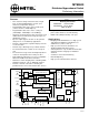
MT90840 Distributed Hyperchannel Switch Preliminary Information Features Output Mux & Drivers PDo7 Applications • • • • • • Bridging ST-BUS/MVIP buses to high speed Time Division Multiplexed backplanes at SONET rates (STS-1, STS-3) High speed isochronous backbones for distributed PBX and LAN systems Switch platforms of up to 2430 channels with guaranteed frame integrity for wideband channels Serial bus control and monitoring Data multiplexing High speed communications interface 8 8 2430 Positi
MT90840 76 78 80 82 84 2 4 6 12 8 VDD STi0 STi1 STi2 STi3 STi4 STi5 STi6 STi7 C4/8R1 F0i/o C4/8R2 VSS VDD NC NC CTo3 CTo2 CTo1 CTo0 10 VSS NC IC RES IRQ DTA CS AS/ALE DS/RD VDD VSS R/W AD7 AD6 AD5 AD4 AD3 AD2 AD1 AD0 VDD Preliminary Information 14 72 16 70 18 68 20 64 52 54 NC NC NC NC NC VDD VSS CTo0 CTo1 CTo2 CTo3 VDD VSS C4/8R2 F0i/o C4/8R1 STi7 STi6 STi5 STi4 STi3 STi2 STi1 STi0 VDD VSS NC NC NC NC VDD PDo7 PDo6 PDo5 PDo4 PDo3 PDo2 PDo1 PDo0 PPFTi/o VSS VDD PDi7 PDi6 PDi5 PDi4
MT90840 Preliminary Information Pin Description Pin # Name Description 43 DS/RD Data Strobe/Read (Input). In Motorola multiplexed-bus mode this pin is DS, an active high input which works with CS to enable read and write operation. In Intel/ National multiplexed-bus mode this pin is RD, an active low input which enables a read-cycle and configures the data bus lines (AD0-AD7) as outputs. 4 44 AS/ALE Address Strobe / Address Latch Enable (Input).
MT90840 Preliminary Information Pin Description (continued) Pin # 84 100 22 66 Name F0i/o Description Serial Port Frame Synchronization (Bidirectional). This 8 kHz frame pulse signal indicates the TDM 125 µsec frame boundary on the serial data port. This pin is compatible with both ST-BUS/MVIP and GCI formatted framing signals.
MT90840 Preliminary Information Pin Description (continued) Pin # Name Description 84 100 59 10 TRST Test Reset (Input). Asynchronously initializes the JTAG TAP controller, placing it in the Test-Logic-Reset state. This pin is pulled high internally when not driven. This pin should be pulsed low on power-up, or held low continuously, to ensure that the MT90840 is in the normal functional state, and not the test state. 60 11 TCK Test Clock (Input). Provides the clock to the JTAG test logic.
MT90840 Functional Description The MT90840 Distributed Hyperchannel Switch is a large switching, multiplexing, and rate-adapting device. The MT90840 bridges serial-bus telecom components, using the Mitel ST-BUS or other industry-standard serial buses, onto a higher speed “backbone”. Mixed data, voice and video signals can be time-interchanged or multiplexed from serial Time Division Multiplexed (TDM) streams onto a high speed parallel bus.
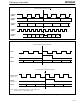
MT90840 Preliminary Information Frame Boundary Established by F0 C4/8R1&2 (4 MHz) Serial I/O 2 Mbps Serial I/O 4 Mbps Ch. 31 Bit 1 Ch. 63 Bit 2 Ch. 31 Bit 0 Ch. 63 Bit 1 Ch. 63 Bit 0 Ch. 0 Bit 6 Ch. 0 Bit 7 Ch. 0 Bit 7 Ch. 0 Bit 6 Ch. 0 Bit 5 C4/8R1&2 (8 MHz) Serial I/O 8 Mbps ch.127 ch.127 ch.127 ch.127 b1 b3 b0 b2 ch. 0 b6 ch. 0 b7 ch. 0 b5 ch. 0 b4 Figure 3 - Serial Port Interface Functional Timing Frame Boundary Established by PPFRi PCKR PPFRi Ch. n-2 PDi0-7 Ch. n-1 Ch.
MT90840 Preliminary Information an address-value in the path’s Data Memory. A given output time slot is controlled by programming the Connection Memory control-address with the address-value of the source input time slot. At the same control-address the output time slot is enabled or tri-stated and other per-channel functions set up. Thus each output time slot is individually controlled, and any given input time slot might be copied to one, several, or none of the output time slots.
Preliminary Information programmed to switch parallel inputs to parallel outputs. For each parallel output channel control-address, the Tx Path Connection Memory is programmed with the 12-bit address-value of the desired parallel input channel. MT90840 specific time slot in an output stream (e.g. STo0-channel7) is programmed in the Rx Path Connection Memory as an input, the corresponding time slot on the equivalent input stream (i.e. STi0-channel7) is automatically an output.
MT90840 Register enables the internal divider, and the SPCKo output (and internal 4.096 MHz clocks) are driven by the clock divided-down from PCKR. At 16.384 MHz, this is a simple divide-by-4, and the SPCKo output jitter will depend on the PCKR input jitter. At 19.44 MHz, the SPCKo output jitter will be larger as the divider switches between rising and falling edges of PCKR. The serial port timing and F0o frame pulse are tightly slaved to PPFRi when INTCLK is set high.
MT90840 Preliminary Information The PPFTi framing in TM1 with PFDI=1 operates similarly, using PCKT, but the PPCE interrupt does not monitor PPFTi. Instead, the TXPAA bit indicates that the PPFTi input is out of phase with F0i. • TM4/Parallel Switching: 2430 (or 2048) channel switching from PDi to PDo. The TM1-0 bits in the TIM Register are used to select the timing modes. The PFDI and SFDI bits in the same register can be used to enable parallel-device sub-modes of TM1 and TM2 respectively.
MT90840 Preliminary Information TM1. This allows for flexible round-trip data delays in star or ring type networks. An elastic buffer on the receive parallel port compensates for the difference in phase between PPFRi/PCKR and F0i/C4. The elastic buffer can also tolerate up to 50 µsec +/- 25 µsec) of clock drift and jitter before the buffer re-syncs and Rx Path data is corrupted. (Data corruption is flagged by the FSA interrupt source.
MT90840 Preliminary Information The transmit path does not provide an elastic buffer, and therefore the serial port clock must be tightly locked (in frequency) to the parallel port clock (PCKR). (Jitter less than +/- 100nsec.) This may be achieved in one of two ways: use of the internal clock divider (INTCLK set high), or use of an external PLL or DPLL, with C4 phase-correction performed by the MT90840. Internal 4.096 MHz Clock Divider For TM2 applications at 19.44 or 16.
MT90840 Preliminary Information CPU MT90840 8 kHz TX 8 8 8 kHz Source PPFT SFDI = 0 PDo0-7 Data TX Data RX 8 kHz RX TX/RX Clock PCKR STo0-7 4.096 MHz SPCKo C4/8R1 & 2 F0o PDi0-7 PPFRi STi/o 0-7 STi/o 0-7 8 8 STi0-7 ST-BUS Components 8 kHz 4.096 MHz or 8.192 MHz (8.192 MHz) PLL 8 8 C4/8R1 & 2 STi0-7 PPFT PDo0-7 Data TX STo0-7 8 8 PCKR Data RX PDi0-7 PPFRi STi/o 0-7 STi/o 0-7 4.
MT90840 Preliminary Information Clock Reference 8 Parallel Data In 8 kHz RX 8 kHz Source 19.44 or 16.384 MHz (RX) MT90840 PDi0-7 Parallel Data Out 8 PDo0-7 PPFTo TX 8 kHz REF PPFRi PCKR CPU Figure 8 - Timing Mode 4 Configuration Timing Mode 4 (TM4) - Parallel Data Switching Timing Mode 4 is used to provide switching of up to 2430 parallel input channels to the same number of parallel output channels. Parallel TDM data is clocked in at PDi0-7 by PCKR, framed by PPFRi.
MT90840 Mode Preliminary Information Data Rates Minimum Delay Total Throughput Delay TM1, TM2, or TM3 S/P All Dmin = 7.7 µsec Note 1 D = Dmin + 1 frame + Po - Si = 132.7 µsec + Po - Si Min. 7.7 µsec, Avg. 133 µsec, Max. 258 µsec TM1P/S All Dmin = ELDmin = 4.4 µsec Note 2 D = 1 frame + ELD + So - Pi = 125 µsec + ELD + So - Pi Min. 4.4 µsec, Max. 379 µsec TM2 P/S All Dmin = 4.3 µsec Note 1 D = Dmin + 1 frame + So - Pi = 129.3 µsec + So - Pi Min. 4.3 µsec, Avg. 129 µsec, Max.
MT90840 Preliminary Information Output Frame Boundary Established by PPFT PPFT PDo7-0 Byte Timing CTo0-3 Outputs Channel 2428 TPCM High, CTn bit address 2428 Channel 2429 Channel 0 Channel 1 TPCM High, CTn bit address 2429 TPCM High, CTn bit address 0 TPCM High, CTn bit address 1 Note: For applications at 16.384 and 6.48 Mbyte/s, only 2048 and 810 positions are usable, in the TPCM. Figure 9 - Parallel Port Control Outputs, CTo0-3 DC=0 for STo 0 channel 1 STi0 O/P I/P .....
MT90840 all 16 serial streams can be individually controlled, so that up to 512 channels can be either transmitted or received. As an example, if all DC bit locations of RPCM High are set HIGH, all 512 channels on STo0-7 and STi0-7 will be configured as outputs. If all DC bits are LOW, then all 512 channels will be configured as inputs. In Add/Drop mode all 512 serial channels are copied into the Transmit Path Data Memory, as inputs, regardless of the DC or OE bits.
MT90840 Preliminary Information Serial I/O Channel TPDM Address STi0, Ch0 000H STi0, Ch1 .. 001H STi7, Ch30 0FEH STi7, Ch31 0FFH STo0 (STi8), Ch0 100H STo0 (STi8), Ch1 101H .. CPU Port Addressing: CAR Address Bus 1 0 6 5 4 3 2 1 0 Stream Channel Serial Input Channel TPCM Contents: 8 7 6 5 mode. Each of the 512 output channels has a control-address in the RPCM. CPU accesses require the 2 LSBs of the CAR Register, and the 7 LSBs of the address bus.
MT90840 Serial Input Channel Preliminary Information TPDM Address STi0, Ch0 000H STi0, Ch1 001H CPU Port Addressing: .. CAR 1 0 STi3, Ch126 1FEH STi4, Ch127 1FFH Stream Note that if the parallel port clocks PCKR & PCKT or serial port clocks C4/8R1 & C4/8R2 are not present during an internal memory access, the DTA output signal may be held HIGH until the clocks are applied again.
MT90840 Preliminary Information A7 A3 A2 A1 A0 # Type LOCATION Reset Value (Hex) 0 0 0 0 0 0 R/W IMS Register 60 0 0 0 0 1 1 R/W Control Register 00 0 0 0 1 0 2 R/W TIM Register 00 0 0 0 1 1 3 R/W GPM Register 00 0 0 1 0 0 4 R/W ALS Register 0X 0 0 1 0 1 5 R/W Test (leave 00hx) 00 0 0 1 1 0 6 - reserved 0 0 1 1 1 7 - reserved 0 1 0 0 0 8 RO Phase Status (Low byte) XX 0 1 0 0 1 9 RO Phase Status (High 3 bits) 0X
MT90840 the DTA pin will be asserted (as the data is stored in the write-pipeline) but the next CPU access will not see DTA asserted. No clocks are necessary for register accesses (but if the write-pipeline is hung, the registers cannot be accessed). If the MT90840 is hung due to a CPU read of a memory with a missing clock, the hang can be cleared by ending the read access.
MT90840 Preliminary Information DR1-0 and FDC in the IMS register) before programming the RPCM. b) The GPM Register is written. The CPU sets the Block-Programming Enable (BPE) bit to HIGH and the Block-Programming Data (BPD7-4) bits to the desired value. This action causes the contents of the BPD7-4 bits to be loaded into the four most significant bits of all addresses in TPCM High, or RPCM High (as set by the Control Register).
MT90840 Preliminary Information I/O pin of the IC. The operation of the boundary-scan circuitry is controlled by a Test Access Port (TAP) Controller. • The Test Data Output (TDO) Serial data is shifted out on this pin. Depending on the present mode of the TAP controller, data will come from one of: the instruction register, the boundary scan register or the bypass register. TDO is clocked out on the falling edge of TCK. When no data is being shifted, the TDO driver is set to a high-impedance state.
MT90840 Preliminary Information Test Data Registers As specified in the IEEE 1149.1 Standard, the MT90840 JTAG interface contains two test data registers: • The Boundary Scan Register consists of a series of Boundary-Scan Cells arranged to form a scan path around the boundary of the core logic of the MT90840. • The Bypass Register is a single stage shift-register that provides a one-bit path that minimizes the distance for test data shifting from the MT90840’s TDI to its TDO.
MT90840 Preliminary Information Register Description Interface Mode Selection Register (IMS) - READ/WRITE DR1 DR1-0 PPS1 PPS0 ODE 0 0 FDC 7 6 5 4 3 2 1 0 Serial Port Data Rate Selection. Select one of three different data rates at the serial inputs and outputs of the MT90840. DR1 DR0 0 0 0 1 1 0 1 1 PPS1-0 DR0 Data Rate 2.048 Mbps 4.096 Mbps 8.192 Mbps reserved Parallel Port Data Rate Selection. Select one of three different data rates for the parallel port of the MT90840.
MT90840 Preliminary Information General Purpose Mode Register (GPM) - READ/WRITE BPD7 BPD6 BPD5 BPD4 PPFP DIN SPFP BPE 7 6 5 4 3 2 1 0 BPD7-4 Block-Programming Data bits 7-4. These bits carry the value to be loaded into the TPCM-High or RPCM-High memory when the Memory Block-Programming feature is activated.
MT90840 Preliminary Information Control Register (CR) - READ/WRITE SEL2 SEL1 SEL0 HA11 HA10 7 6 5 4 3 HA9 2 HA8 HA7 1 0 This register selects which 128 byte page of which internal memory will be accessed by the CPU when the address bit AD<7> is high. (When address bit AD<7> is low, the control registers are accessed.) SEL2-0 Memory Select bits. Used by the CPU to select the internal memories of the MT90840 for read or write operations.
MT90840 Preliminary Information Internal Memory Description Transmit Path Connection Memory High (TPCM High) - This is an 8-bit x 2430-position memory. OE/ CTo0 PPBY MC CTo1 CTo2/ AB11 CTo3/ AB10 AB9 AB8 7 6 5 4 3 2 1 0 (TX Path CM High) OE/CTo0 Output Enable. Provides per channel tristate control on the parallel port side. It controls the MT90840 parallel output drivers to disable (tristate, when LOW) or enable (when HIGH) the transmission of data from the device.
MT90840 Preliminary Information Receive Path Connection Memory High (RPCM High) - This is a 7-bit x 512-position memory. Used only in TM1, 2, & 3. 7 MC DC OE AB11 AB10 AB9 AB8 6 5 4 3 2 1 0 (RX Path CM High) MC Message Channel: The message channel contents are provided by the CPU in bits AB0-7 in the Rx Path Connection Memory Low. If MC is HIGH, the contents of the corresponding location of RPCM Low are output on this serial port channel.
MT90840 Preliminary Information Applications SONET rates such as 51 (STS-1) or 155 Mbps (STS-3). Distributed Isochronous Network Low latency isochronous backbones provide for the deployment of systems that require cost effective implementation, high bandwidth, predictable data transfer delays and direct synchronization with the wide area network.
MT90840 Preliminary Information synchronization scheme may be used in applications such as the proposed MVIP multi-chassis level 3 interface (MC-3 system) utilizing point-to-point or point-to-multipoint switching connections. When the MT90840 operates in a ring application, the Parallel Data Bypass mode is provided to allow all or part of the received input parallel data to be bypassed to the output parallel port feeding the ring back with the data which is not destined for the local station.
MT90840 Preliminary Information AC Electrical Characteristics - Voltages are with respect to ground (VSS) unless otherwise stated. Characteristics 1 C4/8 Input - Clock Period: 4.096 MHz (2.048 & 4.096 Mbps) 8.192 MHz (8.192 Mbps) Sym SPCKo Output - Clock Period generated from external C4/8 reference (2.048 and 4.096 Mbps) 3 C4/8 Input Clock Width HIGH 4.096 MHz (2.048 & 4.096 Mbps) 8.192 MHz (8.
MT90840 Preliminary Information AC Electrical Characteristics - Voltages are with respect to ground (VSS) unless otherwise stated. Characteristics Sym Units 38 50 26 ns ns ns 40 64 ns ns CL=30pF CL=150pF STo Output Delay from 4.096 MHz C4/8 input (TM1) 52 72 ns ns CL=30pF CL=150pF STo 8.192 Mbps Output Delay from C4/8 input (TM1, 2 & 3; STi/o0-3) 28 43 ns ns CL=30pF CL=150pF 28 41 ns SPCKo CL=30pF SPCKo CL=150pF STi Input Setup Time from C4/8 input edge in TM1 (2.048 and 4.
MT90840 Preliminary Information tfrw Foi input (8 kHz) tfrh tfrs tclk tT tclkh tclkl C4/8R1 (4.096 MHz) tstis STi0-7 bit 0, ch. 31 tstih bit 7, ch. 0 tsod STo0-7 bit 0, ch. 31 bit 7, ch. 0 Serial Port with Negative Polarity F0 (ST-BUS) tclk tt tclkh tclkl C4/8R1 (4.096 MHz) tsod STo0-7 bit 0, ch. 31 bit 6, ch. 0 bit 7, ch. 0 tstis bit 7, ch. 0 bit 0, ch.
MT90840 Preliminary Information F0ooutput (8 kHz) tdf tdf tclk tT tclkh tclkl SPCKo (4.096 MHz) tstis tstih STi0-7 bit 0, ch. 31 bit 7, ch. 0 tsod STo0-7 bit 0, ch. 31 bit 7, ch. 0 Serial Port with Negative Polarity F0 (ST-BUS) tclk tt tclkh tclkl SPCKo (4.096 MHz) tsod STo0-7 bit 6, ch. 0 bit 7, ch. 0 bit 0, ch. 31 tstis STi0-7 tstih bit 7, ch.0 bit 0, ch.31 tdf tdf F0o output (8 kHz) Serial Port with Positive Polarity F0 (GCI) Figure 19 - Serial Port Timing for 2.
MT90840 Preliminary Information tclk tclkh tt tclkl C4/8R1 (4.096 MHz) tsod STo0-7 bit 7, ch. 0 bit 0, ch. 63 tstis STi0-7 bit 6, ch. 0 tstih bit 7, ch. 0 tfrs F0i input (8 kHz) tfrh tfrw Serial Port with Negative Polarity F0 (ST-BUS) tclk tclkh tclkl tt C4/8R1 (4.096 MHz) tsod STo0-7 bit 7, ch. 0 bit 0, ch. 63 tstis STi0-7 bit 6, ch. 0 tstih bit 7, ch.
MT90840 Preliminary Information tclk tclkh tt tclkl SPCKo (4.096 MHz) tsod STo0-7 bit 7, ch. 0 bit 0, ch. 63 tstis STi0-7 bit 6, ch. 0 tstih bit 7, ch. 0 tdf tdf F0o output (8 kHz) F0 Frame Sync with Negative Polarity (SPFP = 0) tclk tclkh tclkl tt SPCKo (4.096 MHz) tsod STo0-7 bit 7, ch. 0 bit 0, ch. 63 tstis STi0-7 bit 6, ch. 0 tstih bit7, ch. 0 tdf tdf F0o output (8 kHz) F0 Frame Sync with Positive Polarity (SPFP = 1) Figure 21 - Serial Port Timing for 4.
MT90840 Preliminary Information tclk tclkh tt tclkl C4/8R1 (8.192 MHz) tsod STo0-7 bit 7, ch. 0 bit 0, ch.127 tstis STi0-7 bit 6, ch. 0 tstih bit 7 tfrh tfrs F0i input (8 kHz) tfrw Note: Polarity of F0i is automatically detected in TM1. Expected polarity of F0i in TM2 (SFDI=1) must be programmed with SPFP bit in GPM register. Figure 22 - Serial Port Timing for 8.
MT90840 Preliminary Information tclk tclkh tt C4/8R1** (8.192 MHz reference) STo0-7 tclkl tsod bit 7, ch. 0 bit 0, ch.127 tstis bit 6, ch. 0 tstih bit 7 STi0-7 tdf tdf F0o output (8 kHz) Frame Sync with Positive Polarity (SPFP = 1) tclk tt tclkh C4/8R1** (8.192 MHz reference) STo0-7 tclkl tsod bit 7, ch. 0 bit 0, ch.127 tstis bit 6, ch. 0 tstih bit 7 STi0-7 tdf tdf F0o output (8 kHz) Frame Sync with Negative Polarity (SPFP = 0) ** In TM2 and TM3 operation at 8.
MT90840 Preliminary Information TCP controls the clock-edge on which the output changes.
MT90840 Preliminary Information tclkh tclkl PCKR tclk tstis tstih Byte 1 Byte 0 PDi0-7 tfs tfh PPFRi Figure 28 - Parallel Port Receive Timing AC Electrical Characteristics - Parallel Data Port Characteristics Min Typ‡ Max Units Test Conditions 1 PCKT/PCKR clock period tclk 50 ns 2 PCKT/PCKR HIGH time tclkh 20 ns 3 PCKT/PCKR LOW time tclkl 20 ns 4 PPFTo output delay from PCKR/PCKT transmit edge tdf 28 30 ns CL=30pF CL=50pF 5 PDo output delay from PCKR/PCKT transmit edg
MT90840 Preliminary Information PCKR PPFRi tdf PPFT TCP = 0 tdf TCP = 1 PPFT Note: For the PPFT depicted above, PPFP = HIGH. If PPFP is LOW, the PPFT line will have negative pulse polarity. Figure 29 - Parallel Port in Timing Mode 4 Ch. 3 Bit 1 STo (4 Mbps) Ch. 3 Bit 0 (4 Mbps) Ch. 4 Bit 7 C4/8R1 or C4/8R2 (ST-BUS Mode) tpv tpv PCKT PPFTo n-2 PDo7-0 n-1 n 0 1 2 Note: The MT90840 will correct phase relation in TM1 by moving PPFTo (by moving F0o in TM2 andTM3).
MT90840 Preliminary Information AC Electrical Characteristics† - Intel/National- HPC Multiplexed Bus Mode Voltages are with respect to ground (VSS) unless otherwise stated.
MT90840 Preliminary Information talw 2.0V ALE 0.8V tads AD0AD7 tadh ADDRESS 2.0V DATA talrd 0.8V tcsrw 2.0V CS 0.8V trst 2.0V RD tcsr tdhr 0.8V 2.0V WR tdhw tcsw 0.8V tdsw talwr tddr trdd takh 2.0V DTA 0.
MT90840 Preliminary Information AC Electrical Characteristics† - Motorola Multiplexed Bus Mode Voltages are with respect to ground (VSS) unless otherwise stated.
MT90840 Preliminary Information DS 2.0V 0.8V trwh trws 2.0V R/W 0.8V tdss tasw tdsh 2.0V 0.8V AS tads AD0-7 WR tdhw tadh 2.0V ADDRESS DATA 0.8V tdhr AD0-13 RD 2.0V ADDRESS DATA 0.8V tcss 2.0V CS 0.8V tcsh tddr takh 2.0V DTA 0.
MT90840 Preliminary Information tmssu tmsh TMS tdih ttclk tdisu TDI ttclkh ttclkl TCK tdod TDO ttrst TRST Figure 34 - Boundary Scan Test Port Timing AC Electrical Characteristics - Boundary-Scan Test Port and RESET Pin Parameter Symbol Min Max Units 1 TCK period width t tclk 100 ns 2 TCK period width LOW ttclkl 40 ns 3 TCK period width HIGH ttclkh 40 ns 4 TDI setup time to TCK rising tdisu 2 ns 5 TDI hold time after TCK rising tdih 33 ns 6 TMS setup time to TCK risi
MT90840 Preliminary Information F A G D1 D2 D H Dim Min Max A 0.165 (4.20) 0.200 (5.08) A1 0.090 (2.29) 0.130 (3.30) D/E 0.185 (30.10) 1.195 (30.35) D1/E1 1.150 1.158 (29.210) (29.413) D2/E2 1.090 (27.69) 1.130 (28.70) F 0.026 (0.661) 0.032 (0.812) G 0.013 (0.331) 0.021 (0.533) E E1 H 0.050 BSC (1.27 BSC) I Notes: 1) Not to scale. 2) Governing dimensions are in millimeters (). 3) Dimensions in inches are not exact. 4) For D & E add for allowable Mold Protrusion 0.010".
MT90840 Notes: 2-280 Preliminary Information