
Specifications

mikroElektronika | Free Online Book | PIC Microcontrollers | Chapter 5: CCP Modules
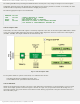
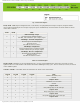
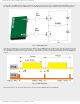
Fig. 5-8 CCP1CON Register
P1M1, P1M0 - PWM Output Configuration bits - In all modes, excepting PWM, the P1A pin is Capture/Compare module
input. P1B, P1C and P1D pins act as input/output port D pins. In PWM mode, these bits affect the CCP1 module as shown
in the table 5-4 below:
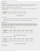
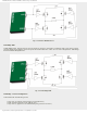
P1M1 P1M0 Mode
0 0
PWM with single output
Pin P1A outputs modulated signal.
Pins P1B, P1C and P1D are port D input/output
0 1
Full Bridge - Forward configuration
Pin P1D outputs modulated signal
Pin P1A is active
Pins P1B and P1C are inactive
1 0
Half Bridge configuration
Pins P1A and P1B output modulated signal
PinsP1C and P1D are port D input/output
1 1
Full Bridge - Reverse configuration
Pin P1B outputs modulated signal
Pin P1C is active
Pins P1A and P1D are inactive
Table 5-4 CCP1CON Register
DC1B1, DC1B0 - PWM Duty Cycle Least Significant bits - are only used in PWM mode in which they represent two least
significant bits of a 10-bit number. This number determines PWM signal’s duty cycle. The rest of bits (8 in total) are stored
in the CCPR1L register.
CCP1M3 - CCP1M0 - CCP1 Mode Select bits determine the mode of the CCP1 module.
CCP1M3 CCP1M2 CCP1M1 CCP1M0 Mode
0 0 0 0 Module is disabled (reset)
0 0 0 1 Unused
0 0 1 0
Compare mode
CCP1IF bit is set on match
0 0 1 1 Unused
0 1 0 0
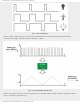
Capture mode
Every falling edge on the CCP1 pin
0 1 0 1
Capture mode
Every rising edge on the CCP1 pin
0 1 1 0
Capture mode
Every 4th rising edge on the CCP1 pin
0 1 1 1
Capture mode
http://www.mikroe.com/en/books/picmcubook/ch5/ (7 of 15)5/3/2009 11:33:21 AM