
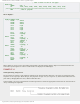
Specifications

mikroElektronika | Free Online Book | PIC Microcontrollers | Appendix B: Examples
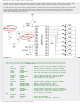
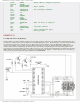
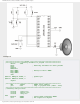
possible, only 8 lower bits of the result of conversion are shown. GND is used as a negative voltage reference Vref-, while
positive voltage reference is applied on the AN3 pin. It enables voltage measurement scale to "stretch and shrink".
To make this clear, the A/D converter always generates a 10-bit binary result, which means that it detects a total of 1024
voltage levels (210=1024). The difference between two voltage levels is not always the same. The less the difference
between Vref+ and Vref, the less the difference will be between two of 1024 levels. Accordingly, the A/D converter is
able to detect slight changes in voltage.
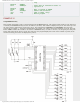
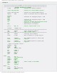
Example 11:
;*********************** Header *********************************************
;************************ PROGRAM START *************************************
org 0x0000 ; Address of the first program instruction
banksel TRISB ; Selects bank containing register TRISB
clrf TRISB ; All port B pins are configured as outputs
movlw B'00001100'
movwf TRISA ; Pins RA2 and RA3 are configured as inputs
banksel ANSEL ; Selects bank containing register ANSEL
movlw B'00001100' ; Inputs AN2 and AN3 are analog while
movwf ANSEL ; all other pins are digital
clrf ANSELH
banksel ADCON1 ; Selects bank including register ADCON1
bsf ADCON1,ADFM ; Right justification of result
bcf ADCON1,VCFG1 ; Voltage Vss is used as Vref
bsf ADCON1,VCFG0 ; RA3 pin voltage is used as Vref+
banksel ADCON0 ; Selects bank containing register ADCON0
movlw B'00001001' ; AD converter uses clock Fosc/2, AD channel
movwf ADCON0 ; on RA2 pin is used for conversion and
; AD converter is enabled
loop
banksel ADCON0
btfsc ADCON0,1 ; Tests bit GO/DONE
goto loop ; Conversion in progress, remain in
http://www.mikroe.com/en/books/picmcubook/appb/ (38 of 54)5/3/2009 11:36:02 AM