
Specifications

mikroElektronika | Free Online Book | PIC Microcontrollers | Chapter 7: Analog Modules
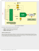
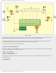
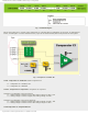
Fig. 7-2 ADRESH and ADRESL Registers
A/D Acquisition Requirements
For the ADC to meet its specified accuracy, it is necessary to provide a certain time delay between selecting specific
analog input and measurement itself. This time is called "acquisition time" and mainly depends on the source impedance.
There is an equation used for accurately calculating this time, which in the worst case amounts to approximately 20uS.
Briefly, after selecting (or changing) the analog input and before starting conversion it is necessary to provide at least
20uS time delay to enable the ACD maximal conversion accuracy.
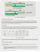
ADC Clock Period
Time needed to complete a one-bit conversion is defined as TAD. The required TAD must be at least 1,6 uS. One full 10-
bit A/D conversion is a bit longer than expected and amounts to 11 TAD periods. However, since both the conversion clock
frequency and source are determined by software, one of the available combination of bits ADCS1 and ADCS0 should be
selected before voltage measurement on some analog input starts. These bits are stored in the ADCON0 register.
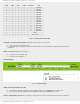
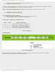
ADC Clock Source ADCS1 ADCS0
Device Frequency (Fosc)
20 Mhz 8 Mhz 4 Mhz 1 Mhz
Fosc/2 0 0 100 nS 250 nS 500 nS 2 uS
Fosc/8 0 1 400 nS 1 uS 2 uS 8 uS
Fosc/32 1 0 1.6 uS 4 uS 8 uS 32 uS
Frc 1 1 2 - 6 uS 2 - 6 uS 2 - 6 uS 2 - 6 uS
Table 7-1 ADC Clock Period
Any change in the system clock frequency will affect the ADC clock frequency, which may adversely affect the ADC result.
Device frequency characteristics are shown in the table above. The values in the shaded cells are outside of recommended
range.
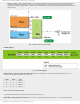
How to Use A/D Converter?
In order to enable the A/D converter to run without problems as well as to avoid unexpected results, it is necessary to
consider the following:
● A/D converter does not differ between digital and analog voltages. In order to avoid errors in measurement or chip
damage, the pins should be configured as analog inputs before conversion starts. The bits used for this purpose are
stored in the TRIS and ANSELH registers;
● When the port with analog inputs marked as CH0-CH13 is read, the corresponding bits will be driven to logic zero
(0); and
http://www.mikroe.com/en/books/picmcubook/ch7/ (3 of 14)5/3/2009 11:34:24 AM