
Specifications

mikroElektronika | Free Online Book | PIC Microcontrollers | Chapter 6: Serial Communication Modules
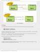
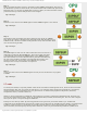
Step 1.
Data to transmit should be written to the buffer register SSPBUF. Immediately after that, if
the SPI module operates in master mode, the microcontroller will automatically perform the
following steps 2, 3 and 4. If the SPI module operates as Slave, the microcontroller will not
perform these steps until the SCK pin detects clock signal.
Fig. 6-15 Step 1
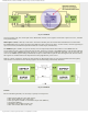
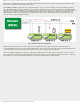
Step 2.
This data is now moved to the SSPSR register and the SSPBUF register is not cleared.
Fig. 6-16 Step 2
Step 3.
Synchronized with clock signal, this data is shifted to the output pin (MSB bit
first) while the register is simultaneously being filled with bits through input pin.
In Master mode, the microcontroller itself generates clock, while the Slave mode
uses external clock (pin SCK).
Fig. 6-17 Step 3
Step 4.
The SSPSR register is full once the 8 bits of data have been received. It is
indicated by setting the BF and SSPIF bits. The received data (that byte)
is automatically moved from the SSPSR register to the SSPBUF register.
Since data transfer via serial communication is performed automatically,
the rest of the program is normally executed while data transfer is in
progress. In that case, the function of the SSPIF bit is to generate
interrupt when one byte transmission is completed.
Fig. 6-18 Step 4
Step 5.
At last, the data stored in the SSPBUF register is ready for use and moved to any register
available.
Fig. 6-19 Step 5
I²C mode
I²C mode (Inter IC Bus) is especially suitable when the microcontroller and integrated circuit, which the microcontroller
should exchange data with, are within the same device. It is commonly about another microcontrollers or specialized,
cheap integrated circuits belonging to the new generation of so called "smart peripheral components" (memories,
temperature sensors, real-time clocks etc.)
Similar to serial communication in SPI mode, data transfer in I²C mode is synchronous and bidirectional. This time only
two pins are used for data transfer. These are the SDA (Serial Data) and SCL (Serial Clock) pins. The user must configure
these pins as inputs or outputs through the TRISC bits.
Perhaps it is not directly visible. By observing particular rules (protocols), this mode enables up to 122 different
components to be simultaneously connected in a simple way by using only two valuable I/O pins. Briefly, everything works
as follows: Clock necessary to synchronize the operation of both devices is always generated by the master device
(microcontroller) and its frequency directly affects baud rate. There are protocols allowing maximum 3,4 MHz clock
http://www.mikroe.com/en/books/picmcubook/ch6/ (16 of 27)5/3/2009 11:33:59 AM