
User manual


Table Of Contents
- CHAPTER 1
- CHAPTER 2
- mikroC PRO for PIC32
- Environment
- Main Menu Options
- File
- Edit
- View
- Project
- Build
- Run
- Tools
- Help
- mikroC PRO for PIC32 IDE
- Code Editor
- Code Explorer
- Project Manager
- Project Settings
- Library Manager
- Routine List
- Statistics
- Messages Window
- Quick Converter
- Macro Editor
- Image Preview
- Toolbars
- Customizing IDE Layout
- Options
- Integrated Tools
- Active Comments
- Export Project
- Jump To Interrupt
- Regular Expressions
- Keyboard Shortcuts
- CHAPTER 3
- CHAPTER 4
- CHAPTER 5
- CHAPTER 6
- CHAPTER 7
- CHAPTER 8
- mikroC PRO for PIC32 Language Reference
- Lexical Elements Overview
- Whitespace
- Comments
- Tokens
- Constants
- Integer Constants
- Floating Point Constants
- Character Constants
- String Constants
- Enumeration Constants
- Pointer Constants
- Constant Expressions
- Keywords
- Identifiers
- Punctuators
- Concepts
- Objects
- Scope and Visibility
- Name Spaces
- Duration
- Types
- Fundamental Types
- Arithmetic Types
- Enumerations
- Void Type
- Derived Types
- Arrays
- Pointers
- Pointer Arithmetic
- Structures
- Working with Structures
- Structure Member Access
- Unions
- Bit Fields
- Types Conversions
- Standard Conversions
- Explicit Types Conversions (Typecasting)
- Declarations
- Linkage
- Storage Classes
- Type Qualifiers
- Typedef Specifier
- asm Declaration
- Initialization
- Functions
- Function Calls and Argument Conversions
- Ellipsis (‘...’) Operator
- Operators
- Arithmetic Operators
- Relational Operators
- Bitwise Operators
- Logical Operators
- Conditional Operator ? :
- Assignment Operators
- Unary Operators
- Sizeof Operator
- Expressions
- Comma Expressions
- Statements
- Labeled Statements
- Expression Statements
- Selection Statements
- If Statement
- Switch Statement
- Iteration Statements (Loops)
- Do Statement
- For Statement
- Jump Statements
- Break and Continue Statements
- Goto Statement
- Return Statement
- Compound Statements (Blocks)
- Preprocessor
- Preprocessor Directives
- Macros
- File Inclusion
- Preprocessor Operators
- Conditional Compilation
- CHAPTER 9
- mikroC PRO for PIC32 Libraries
- Hardware Libraries
- Standard ANSI C Libraries
- Miscellaneous Libraries
- Hardware Libraries
- ADC Library
- CANSPI Library
- Library Dependency Tree
- External dependencies of CANSPI Library
- Library Routines
- CANSPISetOperationMode
- CANSPIGetOperationMode
- CANSPIInitialize
- CANSPISetBaudRate
- CANSPISetMask
- CANSPISetFilter
- CANSPIRead
- CANSPIWrite
- CANSPI Constants
- CANSPI_OP_MODE Constants
- CANSPI_CONFIG_FLAGS Constants
- CANSPI_TX_MSG_FLAGS Constants
- CANSPI_RX_MSG_FLAGS Constants
- CANSPI_MASK Constants
- CANSPI_FILTER Constants
- Library Example
- HW Connection
- Compact Flash Library
- Library Dependency Tree
- External dependencies of Compact Flash Library
- Library Routines
- Cf_Init
- Cf_Detect
- Cf_Enable
- Cf_Disable
- Cf_Read_Init
- Cf_Read_Byte
- Cf_Write_Init
- Cf_Write_Byte
- Cf_Read_Sector
- Cf_Write_Sector
- Cf_Fat_Init
- Cf_Fat_QuickFormat
- Cf_Fat_Assign
- Cf_Fat_Reset
- Cf_Fat_Read
- Cf_Fat_Rewrite
- Cf_Fat_Append
- Cf_Fat_Delete
- Cf_Fat_Write
- Cf_Fat_Set_File_Date
- Cf_Fat_Get_File_Date
- Cf_Fat_Get_File_Date_Modified
- Cf_Fat_Get_File_Size
- Cf_Fat_Get_Swap_File
- Library Example
- HW Connection
- Epson S1D13700 Graphic Lcd Library
- External dependencies of the Epson S1D13700 Graphic Lcd Library
- Library Routines
- S1D13700_Init
- S1D13700_Write_Command
- S1D13700_Write_Parameter
- S1D13700_Read_Parameter
- S1D13700_Fill
- S1D13700_GrFill
- S1D13700_TxtFill
- S1D13700_Display_GrLayer
- S1D13700_Display_TxtLayer
- S1D13700_Set_Cursor
- S1D13700_Display_Cursor
- S1D13700_Write_Char
- S1D13700_Write_Text
- S1D13700_Dot
- S1D13700_Line
- S1D13700_H_Line
- S1D13700_V_Line
- S1D13700_Rectangle
- S1D13700_Box
- S1D13700_Rectangle_Round_Edges
- S1D13700_Rectangle_Round_Edges_Fill
- S1D13700_Circle
- S1D13700_Circle_Fill
- S1D13700_Image
- S1D13700_PartialImage
- Flash Memory Library
- Graphic Lcd Library
- Library Dependency Tree
- External dependencies of Graphic Lcd Library
- Glcd_Init
- Glcd_Set_Side
- Glcd_Set_X
- Glcd_Set_Page
- Glcd_Read_Data
- Glcd_Write_Data
- Glcd_Fill
- Glcd_Dot
- Glcd_Line
- Glcd_V_Line
- Glcd_H_Line
- Glcd_Rectangle
- Glcd_Rectangle_Round_Edges
- Glcd_Rectangle_Round_Edges_Fill
- Glcd_Box
- Glcd_Circle
- Glcd_Circle_Fill
- Glcd_Set_Font
- Glcd_Write_Char
- Glcd_Write_Text
- Glcd_Image
- Glcd_PartialImage
- I²C Library
- Keypad Library
- Lcd Library
- Manchester Code Library
- Memory Manager Library
- Multi Media Card Library
- Secure Digital Card
- Secure Digital High Capacity Card
- Library Dependency Tree
- External dependencies of MMC Library
- Library Routines
- Mmc_Init
- Mmc_Read_Sector
- Mmc_Write_Sector
- Mmc_Read_Cid
- Mmc_Read_Csd
- Mmc_Fat_Init
- Mmc_Fat_QuickFormat
- Mmc_Fat_Assign
- Mmc_Fat_Reset
- Mmc_Fat_Read
- Mmc_Fat_Rewrite
- Mmc_Fat_Append
- Mmc_Fat_Delete
- Mmc_Fat_Write
- Mmc_Fat_Set_File_Date
- Mmc_Fat_Get_File_Date
- Mmc_Fat_Get_File_Date_Modified
- Mmc_Fat_Get_File_Size
- Mmc_Fat_Get_Swap_File
- Library Example
- HW Connection
- OneWire Library
- Port Expander Library
- Library Dependency Tree
- External dependencies of Port Expander Library
- Library Routines
- Expander_Init
- Expander_Init_Advanced
- Expander_Read_Byte
- Expander_Write_Byte
- Expander_Read_PortA
- Expander_Read_PortB
- Expander_Read_PortAB
- Expander_Write_PortA
- Expander_Write_PortB
- Expander_Write_PortAB
- Expander_Set_DirectionPortA
- Expander_Set_DirectionPortB
- Expander_Set_DirectionPortAB
- Expander_Set_PullUpsPortA
- Expander_Set_PullUpsPortB
- Expander_Set_PullUpsPortAB
- Library Example
- HW Connection
- PS/2 Library
- PWM Library
- RS-485 Library
- Software I²C Library
- Software SPI Library
- Software UART Library
- Sound Library
- SPI Library
- SPI Ethernet Library
- Library Dependency Tree
- External dependencies of SPI Ethernet Library
- Library Routines
- SPI_Ethernet_Init
- SPI_Ethernet_Enable
- SPI_Ethernet_Disable
- SPI_Ethernet_doPacket
- SPI_Ethernet_putByte
- SPI_Ethernet_putBytes
- SPI_Ethernet_putConstBytes
- SPI_Ethernet_putString
- SPI_Ethernet_putConstString
- SPI_Ethernet_getByte
- SPI_Ethernet_getBytes
- SPI_Ethernet_UserTCP
- SPI_Ethernet_UserUDP
- SPI_Ethernet_getIpAddress
- Ethernet_getGwIpAddress
- SPI_Ethernet_getDnsIpAddress
- SPI_Ethernet_getIpMask
- SPI_Ethernet_confNetwork
- SPI_Ethernet_arpResolve
- SPI_Ethernet_sendUDP
- SPI_Ethernet_dnsResolve
- SPI_Ethernet_initDHCP
- SPI_Ethernet_doDHCPLeaseTime
- SPI_Ethernet_renewDHCP
- Library Example
- HW Connection
- SPI Ethernet ENC24J600 Library
- Library Dependency Tree
- External dependencies of SPI Ethernet ENC24J600 Library
- Library Routines
- SPI_Ethernet_24j600_Init
- SPI_Ethernet_24j600_Enable
- SPI_Ethernet_24j600_Disable
- SPI_Ethernet_24j600_doPacket
- SPI_Ethernet_24j600_putByte
- SPI_Ethernet_24j600_putBytes
- SPI_Ethernet_24j600_putConstBytes
- SPI_Ethernet_24j600_putString
- SPI_Ethernet_24j600_putConstString
- SPI_Ethernet_24j600_getByte
- SPI_Ethernet_24j600_getBytes
- SPI_Ethernet_24j600_UserTCP
- SPI_Ethernet_24j600_UserUDP
- SPI_Ethernet_24j600_getIpAddress
- SPI_Ethernet_24j600_getGwIpAddress
- SPI_Ethernet_24j600_getDnsIpAddress
- SPI_Ethernet_24j600_getIpMask
- SPI_Ethernet_24j600_confNetwork
- SPI_Ethernet_24j600_arpResolve
- SPI_Ethernet_24j600_sendUDP
- SPI_Ethernet_24j600_dnsResolve
- SPI_Ethernet_24j600_initDHCP
- SPI_Ethernet_24j600_doDHCPLeaseTime
- SPI_Ethernet_24j600_renewDHCP
- SPI Graphic Lcd Library
- Library Dependency Tree
- External dependencies of SPI Lcd Library
- Library Routines
- SPI_Glcd_Init
- SPI_Glcd_Set_Side
- SPI_Glcd_Set_Page
- SPI_Glcd_Set_X
- SPI_Glcd_Read_Data
- SPI_Glcd_Write_Data
- SPI_Glcd_Fill
- SPI_Glcd_Dot
- SPI_Glcd_Line
- SPI_Glcd_V_Line
- SPI_Glcd_H_Line
- SPI_Glcd_Rectangle
- SPI_Glcd_Rectangle_Round_Edges
- SPI_Glcd_Rectangle_Round_Edges_Fill
- SPI_Glcd_Box
- SPI_Glcd_Circle
- SPI_Glcd_Circle_FIll
- SPI_Glcd_Set_Font
- SPI_Glcd_Write_Char
- SPI_Glcd_Write_Text
- SPI_Glcd_Image
- SPI_Glcd_PartialImage
- Library Example
- HW Connection
- SPI Lcd Library
- SPI Lcd8 (8-bit interface) Library
- SPI T6963C Graphic Lcd Library
- Library Dependency Tree
- External dependencies of SPI T6963C Graphic Lcd Library
- Library Routines
- SPI_T6963C_config
- SPI_T6963C_writeData
- SPI_T6963C_writeCommand
- SPI_T6963C_setPtr
- SPI_T6963C_waitReady
- SPI_T6963C_fill
- SPI_T6963C_dot
- SPI_T6963C_write_char
- SPI_T6963C_write_text
- SPI_T6963C_line
- SPI_T6963C_rectangle
- SPI_T6963C_rectangle_round_edges
- SPI_T6963C_rectangle_round_edges_fill
- SPI_T6963C_box
- SPI_T6963C_circle
- SPI_T6963C_circle_fill
- SPI_T6963C_image
- SPI_T6963C_PartialImage
- SPI_T6963C_sprite
- SPI_T6963C_set_cursor
- SPI_T6963C_clearBit
- SPI_T6963C_setBit
- SPI_T6963C_negBit
- SPI_T6963C_displayGrPanel
- SPI_T6963C_displayTxtPanel
- SPI_T6963C_setGrPanel
- SPI_T6963C_setTxtPanel
- SPI_T6963C_panelFill
- SPI_T6963C_grFill
- SPI_T6963C_txtFill
- SPI_T6963C_cursor_height
- SPI_T6963C_graphics
- SPI_T6963C_text
- SPI_T6963C_cursor
- SPI_T6963C_cursor_blink
- Library Example
- HW Connection
- T6963C Graphic Lcd Library
- Library Dependency Tree
- External dependencies of T6963C Graphic Lcd Library
- Library Routines
- T6963C_init
- T6963C_writeData
- T6963C_writeCommand
- T6963C_setPtr
- T6963C_waitReady
- T6963C_fill
- T6963C_dot
- T6963C_write_char
- T6963C_write_text
- T6963C_line
- T6963C_rectangle
- T6963C_rectangle_round_edges
- T6963C_rectangle_round_edges_fill
- T6963C_box
- T6963C_circle
- T6963C_circle_fill
- T6963C_image
- T6963C_PartialImage
- T6963C_sprite
- T6963C_set_cursor
- T6963C_clearBit
- T6963C_setBit
- T6963C_negBit
- T6963C_displayGrPanel
- T6963C_displayTxtPanel
- T6963C_setGrPanel
- T6963C_setTxtPanel
- T6963C_panelFill
- T6963C_grFill
- T6963C_txtFill
- T6963C_cursor_height
- T6963C_graphics
- T6963C_text
- T6963C_cursor
- T6963C_cursor_blink
- Library Example
- HW Connection
- TFT Library
- External dependencies of TFT Library
- Library Routines
- TFT_Init
- TFT_Set_Index
- TFT_Write_Command
- TFT_Write_Data
- TFT_Set_Active
- TFT_Set_Font
- TFT_Write_Char
- TFT_Write_Text
- TFT_Fill_Screen
- TFT_Dot
- TFT_Set_Pen
- TFT_Set_Brush
- TFT_Line
- TFT_H_Line
- TFT_V_Line
- TFT_Rectangle
- TFT_Rectangle_Round_Edges
- TFT_Circle
- TFT_Image
- TFT_Partial_Image
- TFT_Image_Jpeg
- TFT_RGBToColor16bit
- TFT_Color16bitToRGB
- HW Connection
- Touch Panel Library
- Touch Panel TFT Library
- UART Library
- USB Library
- Standard ANSI C Libraries
- ANSI C Ctype Library
- ANSI C Math Library
- ANSI C Stdlib Library
- ANSI C String Library
- Miscellaneous Libraries
- Button Library
- Conversions Library
- PrintOut Library
- Setjmp Library
- Sprint Library
- Time Library
- Trigonometry Library
- CHAPTER 10
- Tutorials
- Managing Project
- New Project
- New Project
- Customizing Projects
- Add/Remove Files from Project
- Source Files
- Edit Project
- Source Files
- Clean Project Folder
- Compilation
- Creating New Library
- Frequently Asked Questions
- Can I use your compilers and programmer on Windows Vista (Windows 7) ?
- I am getting “Access is denied” error in Vista, how to solve this problem ?
- What are differences between mikroC PRO, mikroPascal PRO and mikroC PRO compilers ? Why do they have different prices ?
- Why do your PIC compilers don’t support 12F508 and some similar chips ?
- What are limitations of demo versions of mikroElektronika’s compilers ?
- Why do I still get demo limit error when I purchased and installed license key ?
- I have bought license for the older version, do I have to pay license for the new version of the compiler ?
- Do your compilers work on Windows Vista (Windows 7) ?
- What does this function/procedure/routine do ?
- I try to compile one of the provided examples and nothing happens, what is the problem?
- Can I get your library sources ? I need to provide all sources with my project.
- Can I use code I developed in your compilers in commercial purposes ? Are there some limitations ?
- Why does an example provided with your compilers doesn’t work ?
- Your example works if I use the same MCU you did, but how to make it work for another MCU ?
- I need this project finished, can you help me ?
- Do you have some discount on your compilers/development systems for students/professors ?
- I have a question about your compilers which is not listed here. Where can I find an answer ?
mikroC PRO for PIC32
MikroElektronika
307
Epson S1D13700 Graphic Lcd Library
The mikroC PRO for PIC32 provides a library for working with Glcds based on Epson S1D13700 controller.
The S1D13700 Glcd is capable of displaying both text and graphics on an LCD panel. The S1D13700 Glcd allows
layered text and graphics, scrolling of the display in any direction, and partitioning of the display into multiple screens.
It includes 32K bytes of embedded SRAM display memory which is used to store text, character codes, and bit-mapped
graphics.
The S1D13700 Glcd handles display controller functions including:
- Transferring data from the controlling microprocessor to the buffer memory
- Reading memory data, converting data to display pixels
- Generating timing signals for the LCD panel
The S1D13700 Glcd is designed with an internal character generator which supports 160, 5x7 pixel characters in
internal mask ROM (CGROM) and 64, 8x8 pixel characters incharacter generator RAM (CGRAM).
When the CGROM is not used, up to 256, 8x16 pixel characters are supported in CGRAM.
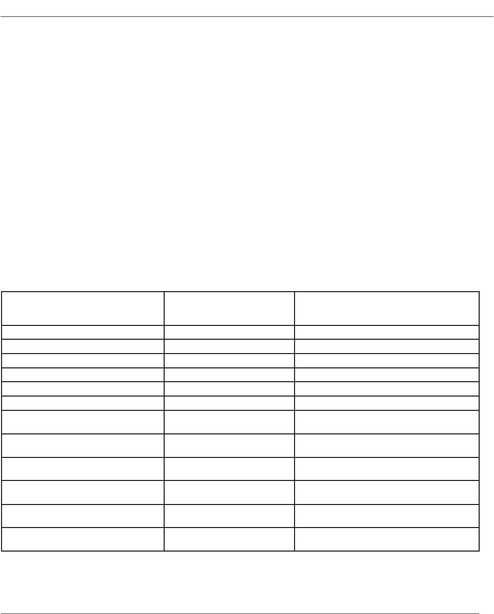
External dependencies of the Epson S1D13700 Graphic Lcd Library
The following variables must be dened
in all projects using S1D13700 Graphic
Lcd library:
Description: Example:
extern sfr char S1D13700_DATA;
System data bus.
char S1D13700_DATA at PORTD;
extern sfr sbit S1D13700_WR;
Write signal.
sbit S1D13700_WR at LATC2_bit;
extern sfr sbit S1D13700_RD;
Read signal.
sbit S1D13700_RD at LATC1_bit;
extern sfr sbit S1D13700_A0;
System Address pin.
sbit S1D13700_A0 at LATC0_bit;
extern sfr sbit S1D13700_RES;
Reset signal.
sbit S1D13700_RES at LATC4_bit;
extern sfr sbit S1D13700_CS;
Chip select.
sbit S1D13700_CS at LATC4_bit;
extern sfr sbit S1D13700_DATA_
Direction;
Direction of the system data bus
pins.
sbit S1D13700_DATA_Direction at
TRISD;
extern sfr sbit S1D13700_WR_
Direction;
Direction of the Write pin.
sbit S1D13700_WR_Direction at TRISC2_
bit;
extern sfr sbit S1D13700_RD_
Direction;
Direction of the Read pin.
sbit S1D13700_RD_Direction at TRISC1_
bit;
extern sfr sbit S1D13700_A0_
Direction;
Direction of the System Address
pin.
sbit S1D13700_A0_Direction at TRISC2_
bit;
extern sfr sbit S1D13700_RES_
Direction;
Direction of the Reset pin.
sbit S1D13700_RES_Direction at
TRISC0_bit;
extern sfr sbit S1D13700_CS_
Direction;
Direction of the Chip select pin.
sbit S1D13700_CS_Direction at TRISC4_
bit;