
Information


PIC18F8722 FAMILY
DS39646C-page 196 © 2008 Microchip Technology Inc.
18.4.4 HALF-BRIDGE MODE
In the Half-Bridge Output mode, two pins are used as
outputs to drive push-pull loads. The PWM output sig-
nal is output on the P1A pin, while the complementary
PWM output signal is output on the P1B pin
(Figure 18-4). This mode can be used for half-bridge
applications, as shown in Figure 18-5, or for full-bridge
applications, where four power switches are being
modulated with two PWM signals.
In Half-Bridge Output mode, the programmable
dead-band delay can be used to prevent shoot-through
current in half-bridge power devices. The value of bits,
P1DC<6:0> sets the number of instruction cycles
before the output is driven active. If the value is greater
than the duty cycle, the corresponding output remains
inactive during the entire cycle. See Section 18.4.6
“Programmable Dead-Band Delay” for more details
on dead-band delay operations.
The P1A and P1B outputs are multiplexed with the
PORTC<2> and PORTE<6> data latches. Alternatively,
P1B can be assigned to PORTH<7> by programming
the ECCPMX Configuration bit to ‘0’. See Table 18-1,
Table 18-2 and Table 18-3 for more information. The
associated TRIS bit must be cleared to configure P1A
and P1B as outputs.
FIGURE 18-4: HALF-BRIDGE PWM
OUTPUT
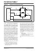
FIGURE 18-5: EXAMPLES OF HALF-BRIDGE OUTPUT MODE APPLICATIONS
Period
Duty Cycle
td
td
(1)
P1A
(2)
P1B
(2)
td = Dead Band Delay
Period
(1) (1)
Note 1: At this time, the TMR2 register is equal to the
PR2 register.
2: Output signals are shown as active-high.
PIC18F6X27/6X22/8X27/8X22
P1A
P1B
FET
Driver
FET
Driver
V+
V-
Load
+
V
-
+
V
-
FET
Driver
FET
Driver
V+
V-
Load
FET
Driver
FET
Driver
PIC18F6X27/6X22/8X27/8X22
P1A
P1B
Standard Half-Bridge Circuit (“Push-Pull”)
Half-Bridge Output Driving a Full-Bridge Circuit