
Information


PIC18F8722 FAMILY
DS39646C-page 194 © 2008 Microchip Technology Inc.
18.4.3 PWM OUTPUT CONFIGURATIONS
The P1M1:P1M0 bits in the CCP1CON register allow
one of four configurations:
• Single Output
• Half-Bridge Output
• Full-Bridge Output, Forward mode
• Full-Bridge Output, Reverse mode
The Single Output mode is the standard PWM mode
discussed in Section 18.4 “Enhanced PWM Mode”.
The Half-Bridge and Full-Bridge Output modes are
covered in detail in the sections that follow.
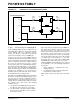
The general relationship of the outputs in all
configurations is summarized in Figure 18-2.
FIGURE 18-2: PWM OUTPUT RELATIONSHIPS (ACTIVE-HIGH STATE)
0
Period
00
10
01
11
SIGNAL
PR2 + 1
CCP1CON<7:6>
P1A Modulated
P1A Modulated
P1B Modulated
P1A Active
P1B Inactive
P1C Inactive
P1D Modulated
P1A Inactive
P1B Modulated
P1C Active
P1D Inactive
Duty
Cycle
(Single Output)
(Half-Bridge)
(Full-Bridge,
Forward)
(Full-Bridge,
Reverse)
Delay
(1)
Delay
(1)
Relationships:
• Period = 4 * T
OSC * (PR2 + 1) * (TMR2 Prescale Value)
• Duty Cycle = T
OSC * (CCPR1L<7:0>:CCP1CON<5:4>) * (TMR2 Prescale Value)
• Delay = 4 * T
OSC * (ECCP1DEL<6:0>)
Note 1: Dead-band delay is programmed using the ECCP1DEL register (Section 18.4.6 “Programmable
Dead-Band Delay”).