
Information


PIC18F8722 FAMILY
DS39646C-page 108 © 2008 Microchip Technology Inc.
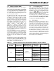
FIGURE 7-10: EXTERNAL MEMORY BUS TIMING FOR SLEEP (MICROPROCESSOR MODE)
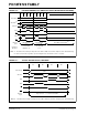
FIGURE 7-11: TYPICAL OPCODE FETCH, 8-BIT MODE
Q2Q1 Q3 Q4 Q2Q1 Q3 Q4
A<19:16>
(1)
ALE
OE
AAh
AD<7:0>
00h
00h
CE
Opcode Fetch
Opcode Fetch
SLEEP
SLEEP
from 007554h
Q1
Bus Inactive
(2)
00h ABh 55h
Memory
Cycle
Instruction
Execution
INST(PC – 2)
Sleep Mode,
MOVLW 55h
from 007556h
AD<15:8>
(1)
3Ah
3Ah
03h
0Eh
BA0
Note 1: The address lines actually used depends on the address width selected. This example assumes 20-bit addressing.
2: Bus becomes inactive regardless of power-managed mode entered when
SLEEP is executed.
Q2Q1 Q3 Q4
AD<15:8>
(1)
ALE
OE
WRL
AD<7:0>
03Ah
BA0
Opcode Fetch
55h0Eh
‘
1’
‘
1’
Memory
Cycle
MOVLW 55h from 007556h
55h
Note 1: The address lines actually used depends on the address width selected. This example assumes 16-bit addressing.