
Datasheet


dsPIC33EPXXX(GP/MC/MU)806/810/814 and PIC24EPXXX(GP/GU)810/814
DS70616F-page 518 Preliminary © 2009-2012 Microchip Technology Inc.
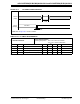
FIGURE 32-10: OC/PWM MODULE TIMING CHARACTERISTICS
TABLE 32-28: OUTPUT COMPARE MODULE TIMING REQUIREMENTS
AC CHARACTERISTICS
Standard Operating Conditions: 3.0V to 3.6V
(unless otherwise stated)
Operating temperature -40°C ≤ TA ≤ +85°C for Industrial
-40°C ≤ T
A ≤ +125°C for Extended
Param. Symbol Characteristic
(1)
Min. Typ. Max. Units Conditions
OC10 TccF OCx Output Fall Time — — — ns See parameter DO32
OC11 TccR OCx Output Rise Time — — — ns See parameter DO31
Note 1: These parameters are characterized but not tested in manufacturing.
OCFA
OCx
OC20
OC15
Active
User-specified Fault State
TABLE 32-29: OC/PWM MODE TIMING REQUIREMENTS
AC CHARACTERISTICS
Standard Operating Conditions: 3.0V to 3.6V
(unless otherwise stated)
Operating temperature -40°C ≤ TA ≤ +85°C for Industrial
-40°C ≤ T
A ≤ +125°C for Extended
Param. Symbol Characteristic
(1)
Min. Typ. Max. Units Conditions
OC15 T
FD Fault Input to PWM I/O
Change
——TCY + 20 ns —
OC20 T
FLT Fault Input Pulse Width TCY + 20 — — ns —
Note 1: These parameters are characterized but not tested in manufacturing.