
Datasheet


© 2009-2012 Microchip Technology Inc. Preliminary DS70616F-page 513
dsPIC33EPXXX(GP/MC/MU)806/810/814 and PIC24EPXXX(GP/GU)810/814
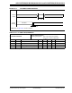
FIGURE 32-5: BOR AND MASTER CLEAR RESET TIMING CHARACTERISTICS
MCLR
(SY20)
BOR
(SY30)
TMCLR
TBOR
Reset Sequence
CPU starts fetching code
Various delays (depending on configuration)
TABLE 32-22: RESET, WATCHDOG TIMER, OSCILLATOR START-UP TIMER, POWER-UP TIMER
TIMING REQUIREMENTS
AC CHARACTERISTICS
Standard Operating Conditions: 3.0V to 3.6V
(unless otherwise stated)
Operating temperature -40°C ≤ TA ≤ +85°C for Industrial
-40°C ≤ TA ≤ +125°C for Extended
Param. Symbol Characteristic
(1)
Min. Typ.
(2)
Max. Units Conditions
SY00 TPU Power-up Period — 400 600 μs
—
SY10 T
OST Oscillator Start-up Time — 1024 TOSC ——TOSC = OSC1 period
SY11 TPWRT Power-up Timer Period — — — — See Section 29.1
“Configuration Bits” and LPRC
specification F21 (Table 32-20)
SY12 TWDT Watchdog Timer
Time-out Period
— — — — See Section 29.4 “Watchdog
Timer (WDT)” and LPRC
specification F21 (Table 32-20)
SY13 T
IOZ I/O High-Impedance
from MCLR
Low or
Watchdog Timer Reset
0.68 0.72 1.2 μs—
SY20 TMCLR MCLR Pulse Width (low) 2 — — μs
—
SY30 T
BOR BOR Pulse Width (low) 1 — — μs—
SY35 T
FSCM Fail-Safe Clock Monitor
Delay
— 500 900 μs -40°C to +85°C
SY36 T
VREG Voltage regulator
standby-to-active mode
transition time
——30µs —
SY37 TOSCDFRC FRC Oscillator start-up
delay
——29µs —
SY38 T
OSCDLPRC LPRC Oscillator start-up
delay
——70µs —
Note 1: These parameters are characterized but not tested in manufacturing.
2: Data in “Typ” column is at 3.3V, 25°C unless otherwise stated.