
Datasheet


dsPIC33EPXXX(GP/MC/MU)806/810/814 and PIC24EPXXX(GP/GU)810/814
DS70616F-page 512 Preliminary © 2009-2012 Microchip Technology Inc.
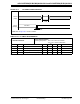
FIGURE 32-4: POWER-ON RESET TIMING CHARACTERISTICS
VDD
VPOR
Note 1: The Power-up period will be extended if the Power-up sequence completes before the device exits from BOR
(V
DD < VBOR).
2: The power-up period Includes internal voltage regulator stabilization delay.
SY00
Power Up Sequence
VDD
VPOR
Power-up Timer Enabled –
Power-up Timer Disabled –
(
TPU
)
SY10
SY11
Power Up Sequence
(Note 1,2)
CPU starts fetching code
CPU starts fetching code
(
TPWRT
)
Clock Sources = (HS, HSPLL, XT, XTPLL and Sosc)
V
DD
VPOR
SY00
Power Up Sequence
Power-up Timer Disabled –
(
TPU
)
CPU starts fetching code
(Note 1,2)
(Note 1,2)
Clock Sources = (FRC, FRCDIVN, FRCDIV16, FRCPLL, EC, ECPLL and LPRC)
Clock Sources = (FRC, FRCDIVN, FRCDIV16, FRCPLL, EC, ECPLL and LPRC)
(
TOST
)
SY00
(
TPU
)
VDD
VPOR
Power-up Timer Enabled –
Greater of
Power Up Sequence
(Note 1,2)
CPU starts fetching code
(
TOST
)
Clock Sources = (HS, HSPLL, XT, XTPLL and Sosc)
SY00
(
TPU
)
SY11
(
TPWRT
)
SY10
or