
Information


Electrical characteristics STM32F405xx, STM32F407xx
142/185 DocID022152 Rev 4
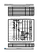
Synchronous waveforms and timings
Figure 59 through Figure 62 represent synchronous waveforms and Table 80 through
Table 82 provide the corresponding timings. The results shown in these tables are obtained
with the following FSMC configuration:
• BurstAccessMode = FSMC_BurstAccessMode_Enable;
• MemoryType = FSMC_MemoryType_CRAM;
• WriteBurst = FSMC_WriteBurst_Enable;
• CLKDivision = 1; (0 is not supported, see the STM32F40xxx/41xxx reference manual)
• DataLatency = 1 for NOR Flash; DataLatency = 0 for PSRAM
In all timing tables, the
T
HCLK
is the HCLK clock period (with maximum
FSMC_CLK = 60 MHz).
t
h(NE_NWE)
FSMC_NWE high to FSMC_NE high hold time T
HCLK
-ns
t
v(A_NE)
FSMC_NEx low to FSMC_A valid - 0 ns
t
v(NADV_NE)
FSMC_NEx low to FSMC_NADV low 1 2 ns
t
w(NADV)
FSMC_NADV low time T
HCLK
– 2 T
HCLK
+ 1 ns
t
h(AD_NADV)
FSMC_AD(address) valid hold time after
FSMC_NADV high)
T
HCLK
–2 - ns
t
h(A_NWE)
Address hold time after FSMC_NWE high T
HCLK
-ns
t
h(BL_NWE)
FSMC_BL hold time after FSMC_NWE high T
HCLK
–2 - ns
t
v(BL_NE)
FSMC_NEx low to FSMC_BL valid - 1.5 ns
t
v(Data_NADV)
FSMC_NADV high to Data valid - T
HCLK
–0.5 ns
t
h(Data_NWE)
Data hold time after FSMC_NWE high T
HCLK
-ns
1. C
L
= 30 pF.
2. Based on characterization, not tested in production.
Table 78. Asynchronous multiplexed PSRAM/NOR write timings
(1)(2)